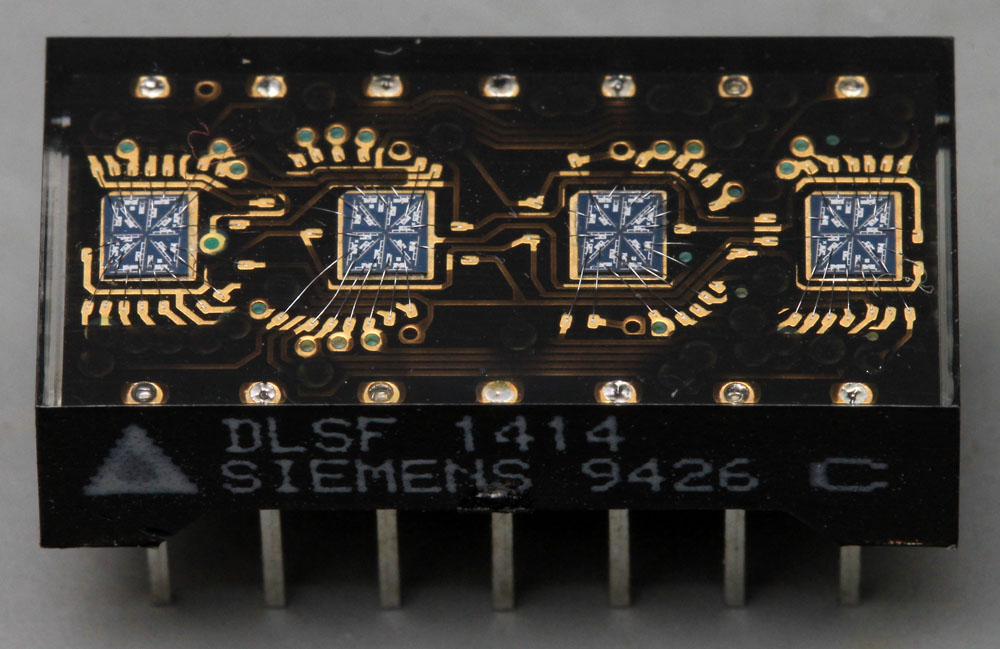
DLSF1414, a strange 4* 16 segment display built by Siemens. You can´t find any information regarding the DLSF1414. There was just a DL1414 but Siemens did customer specific displays too. Perhaps the DLSF1414 is such a customer specific display.
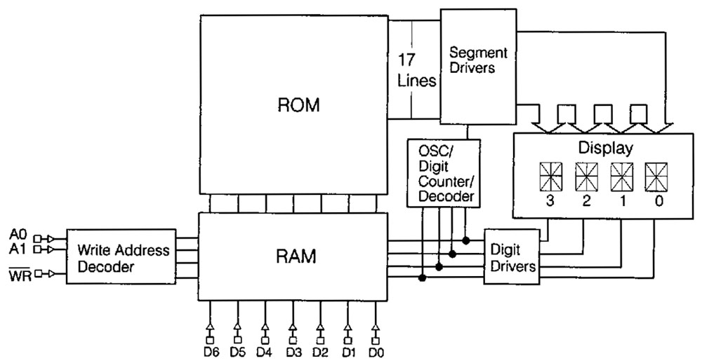
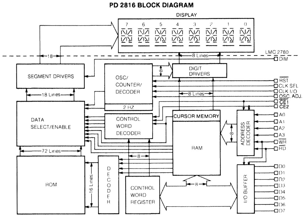
The DL1414 contains a RAM which is adressed with two adress bits and a write input. Through a 7Bit interface you put the code of the character you want to see into one of the four slots of the RAM.
There is an oscillator that activates one digit after the other. While activating a digit the circuit activates one of the slots in the RAM. The RAM outputs the saved code to the ROM and the ROM outputs 17Bits that activates the segments that show the character we wanted to see.
There are other displays that provide you with more functions. Perhaps the DLSF1414 is a DL1414 with some of these functions added.
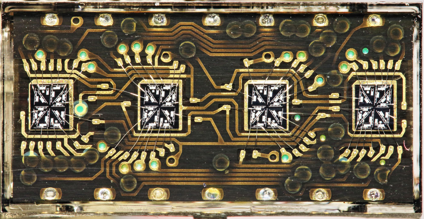
In the DLSF1414 there is a board potted in clear potting.
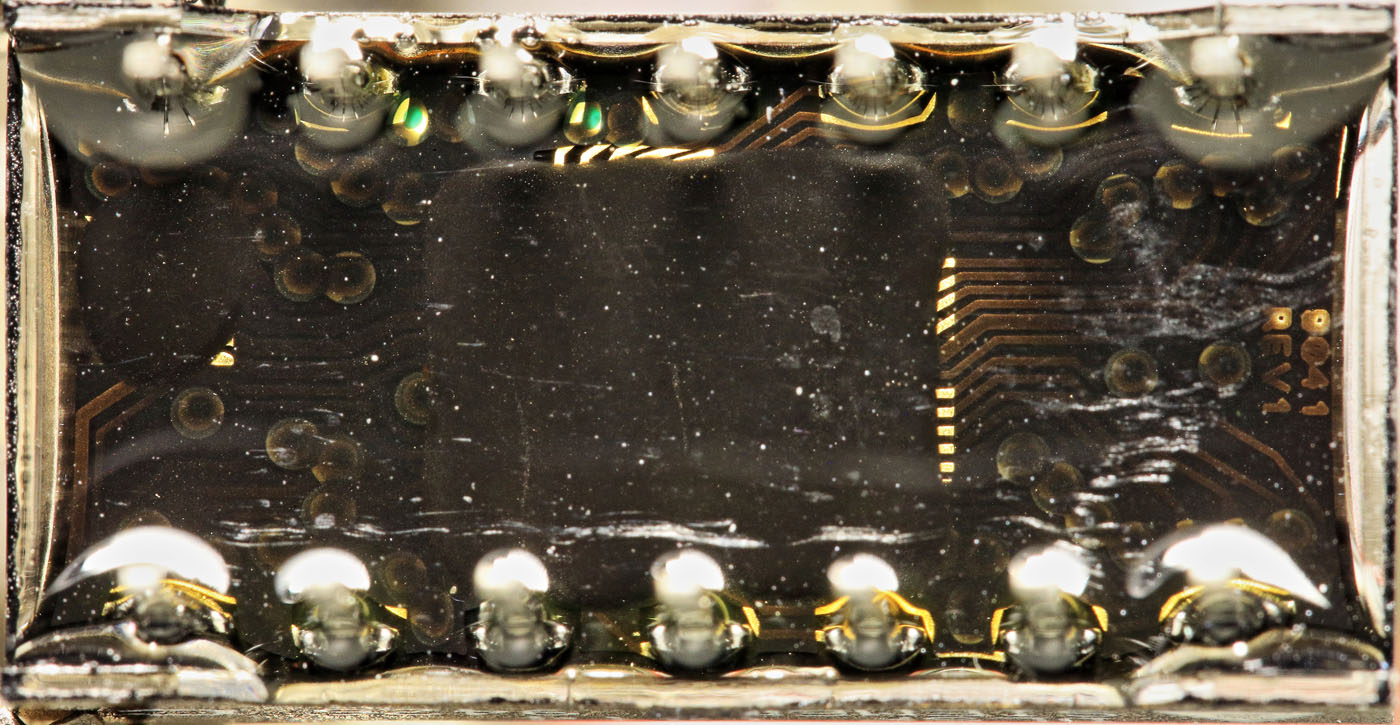
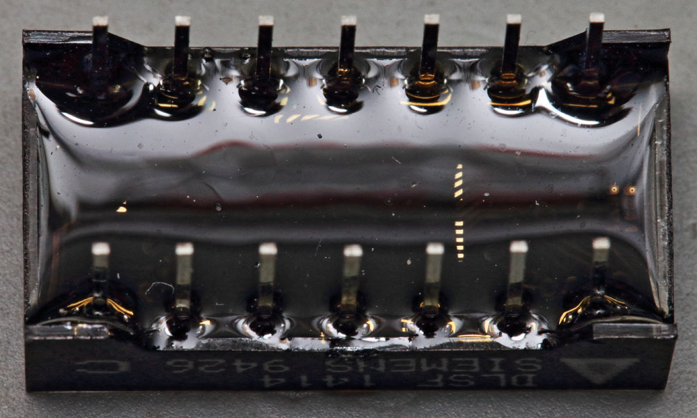
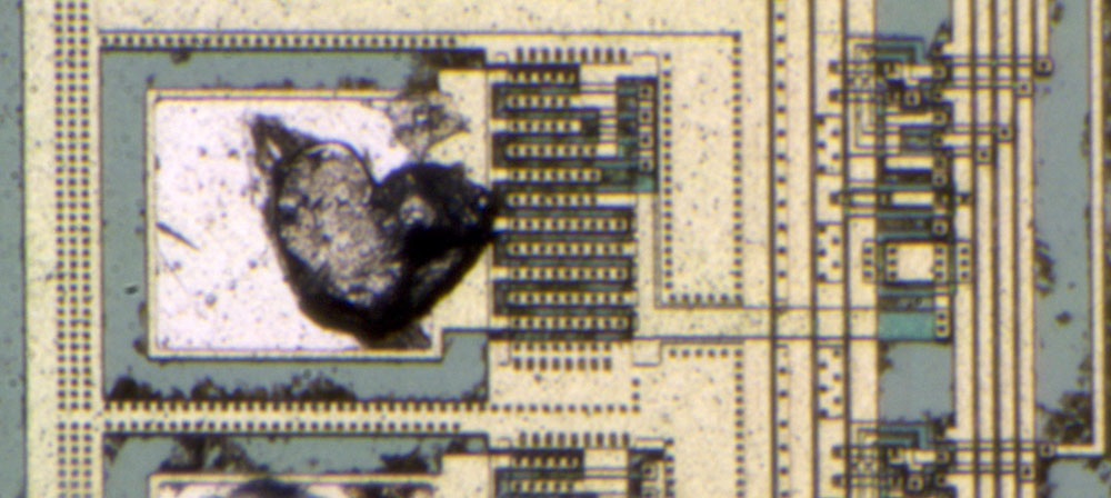
On the backside we see the control circuit that is potted with some dark potting. There seems to be a second circuit in the upper left corner. Perhaps that´s a small logic circuit and that is the difference between the DL1414 and the DLSF1414. (This circuit is lost.

)
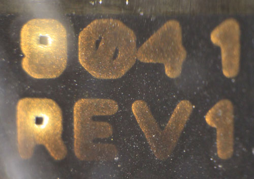
9041, probably the datecode.
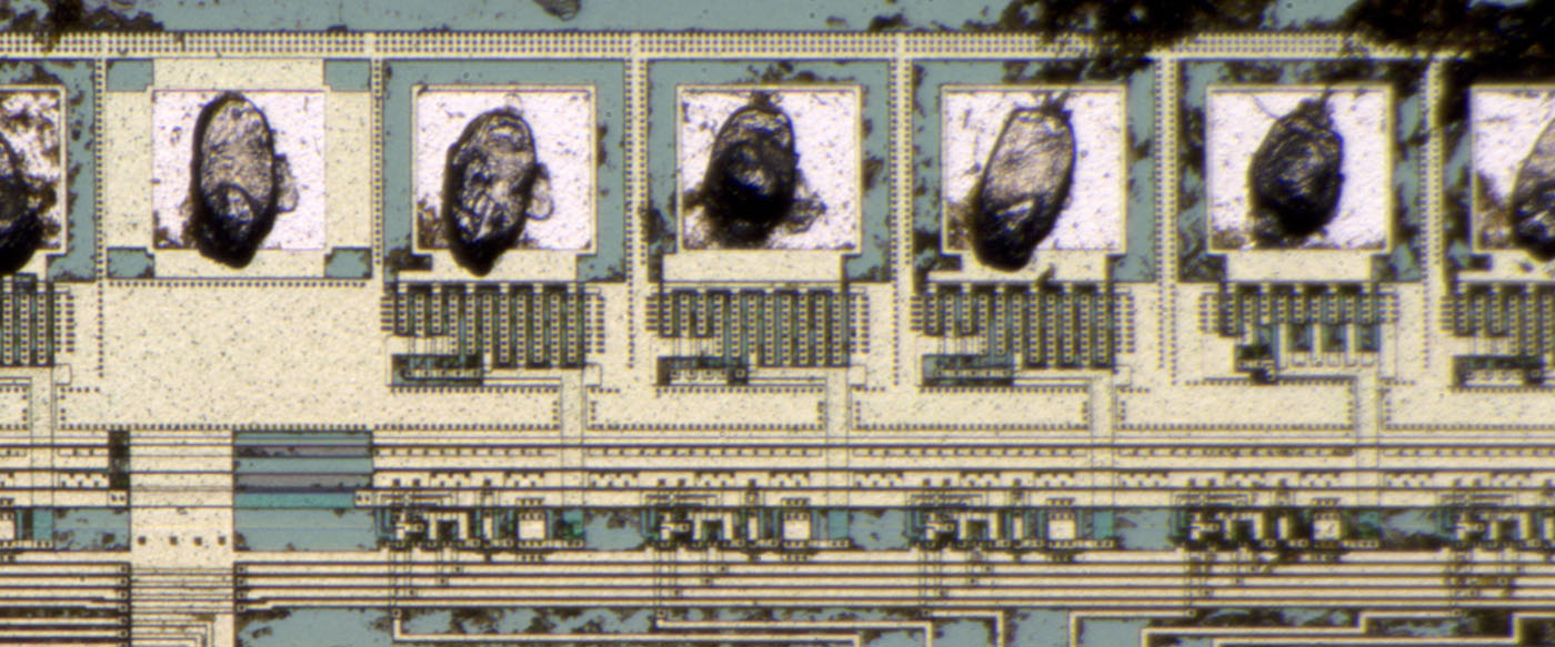
The digits are dies with the dimensions 2,1mm x 1,8mm. There are 16 segments and a dot.
Since there is a dot at the upper edge and at the lower edge you can bond the die rotated 180°.
Thin metal lines distribute the current over the light emitting segments. The substrate is the common anode.
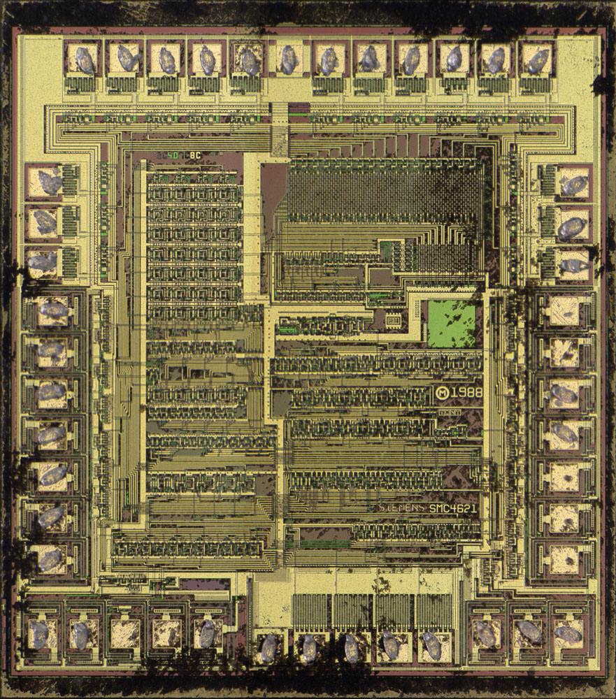
The control circuit is 3,1mm x 2,7mm.
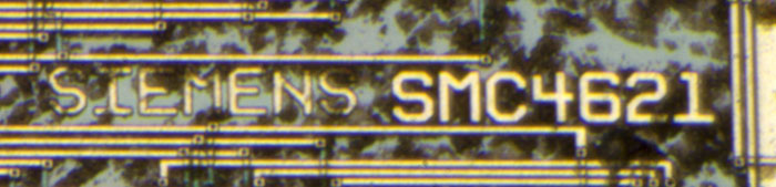
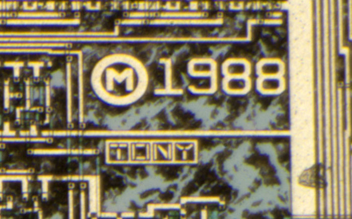
Siemens designed the control circuit in 1988. SMC4621 probably is a internal naming.
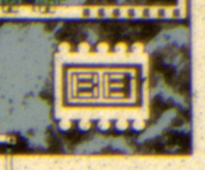
TONY? BE?

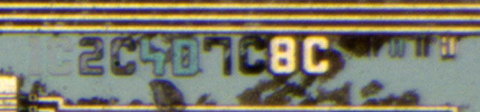
We can find five mask revisions: 1C, 2C, 4D, 7C, 8C
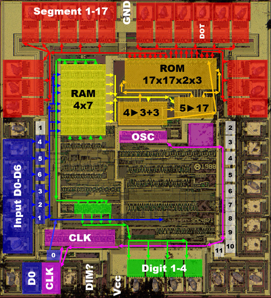
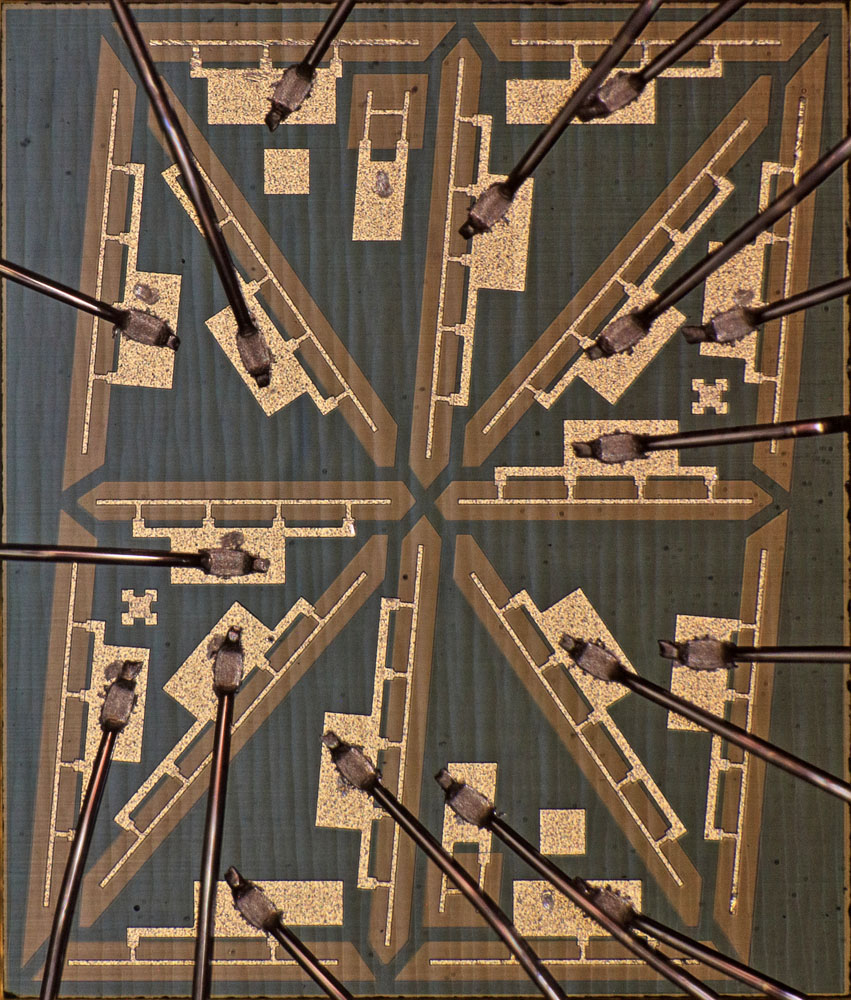
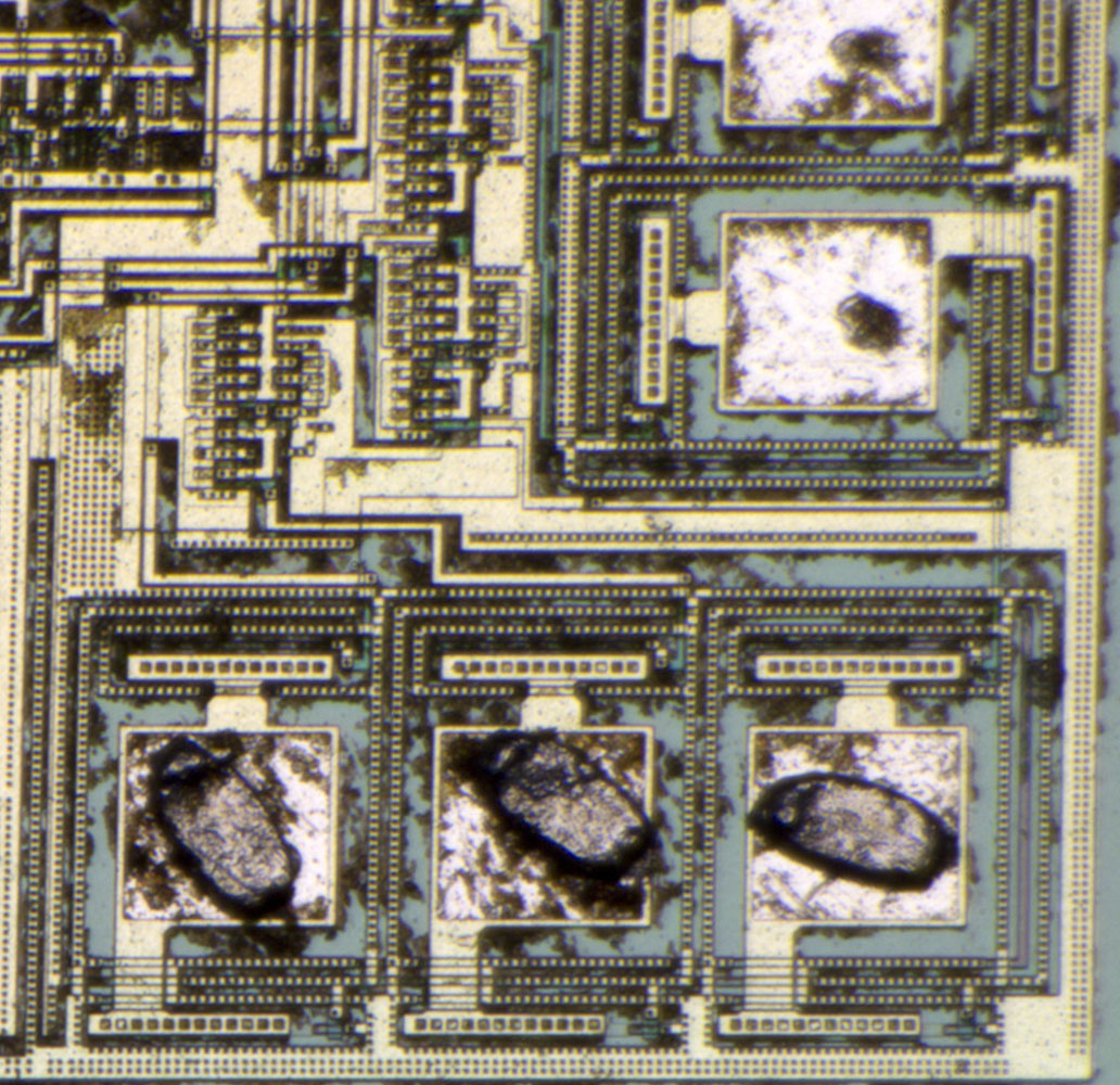
Some areas are easy to spot. At the upper edge there are 17 driver for 16 segments and a dot (red). At the lower edge there are four driver for the four digits (green).
At the left edge we can find the data interface (blue). There are seven bondpads side by side but D0 is placed at the bottom of the die. There are buffer stages as shown in the block diagram.
The data interface is connected to a 4x7 RAM (yellow). The control lines for the four columns of the RAM are connected to the digit drivers (green). You activate one column and the digit drivers activate the right digit (over a small logic).
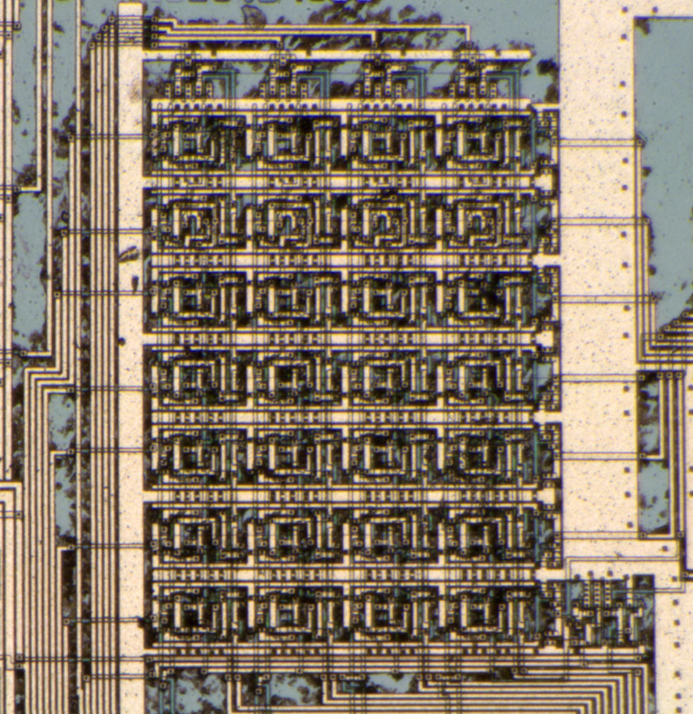
The output of the RAM is the input for the ROM with a quite complex signal conditioning (orange). The size of the ROM is best explained with 17x17x2x3. The output of the ROM is connected to the segment drivers.
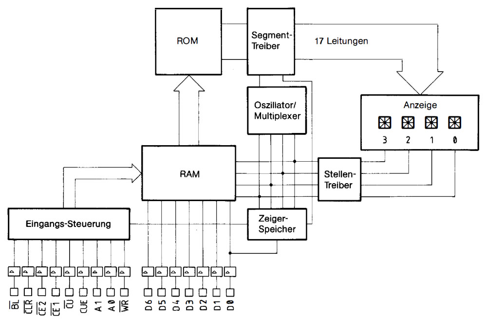
In the middle of the die we can spot an oscillator with a big capacitor (pink). The clock is fed to a bondpad and from there to something like a clock divider and distribution. It seems like the control circuit can be used for other displays with more functionality. As seen in the block diagrams there are displays with a clock input/output. One bondpad is directly connected to the segment drivers. Perhaps that one was used for dimming the display. There are some more used and unused bondpads eleven of them are equipped with buffer stages as the data interface.
Here we see a segment driver. There is a big transistor right of the bondpad and a control circuit right of the transistor. There has to be some current limiting.
The power transistor for the small dot is smaller than for the other segments as it has to sink less current for the same brightness.
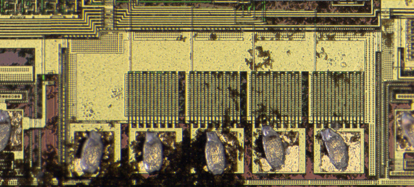
The digit drivers are bigger but less complex.
Above and below the input bondpads there are protection circuits.
Here we have the 4x7 RAM. Left the input, right the output.
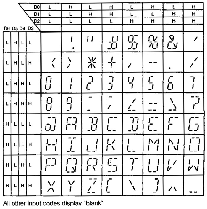
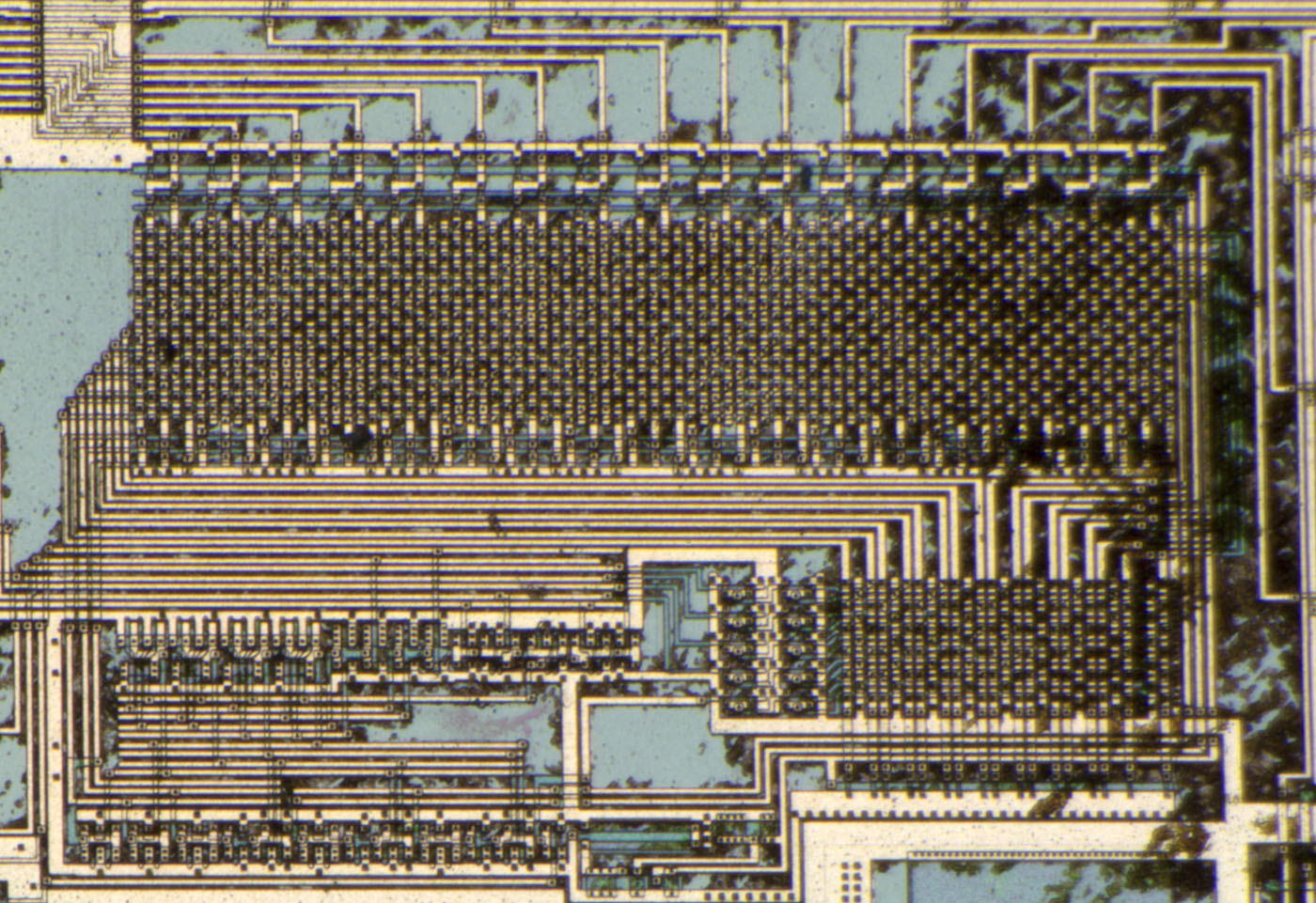
The ROM has to contain 63 characters. So you need a 17x63 ROM. But that ROM looks quite strange...
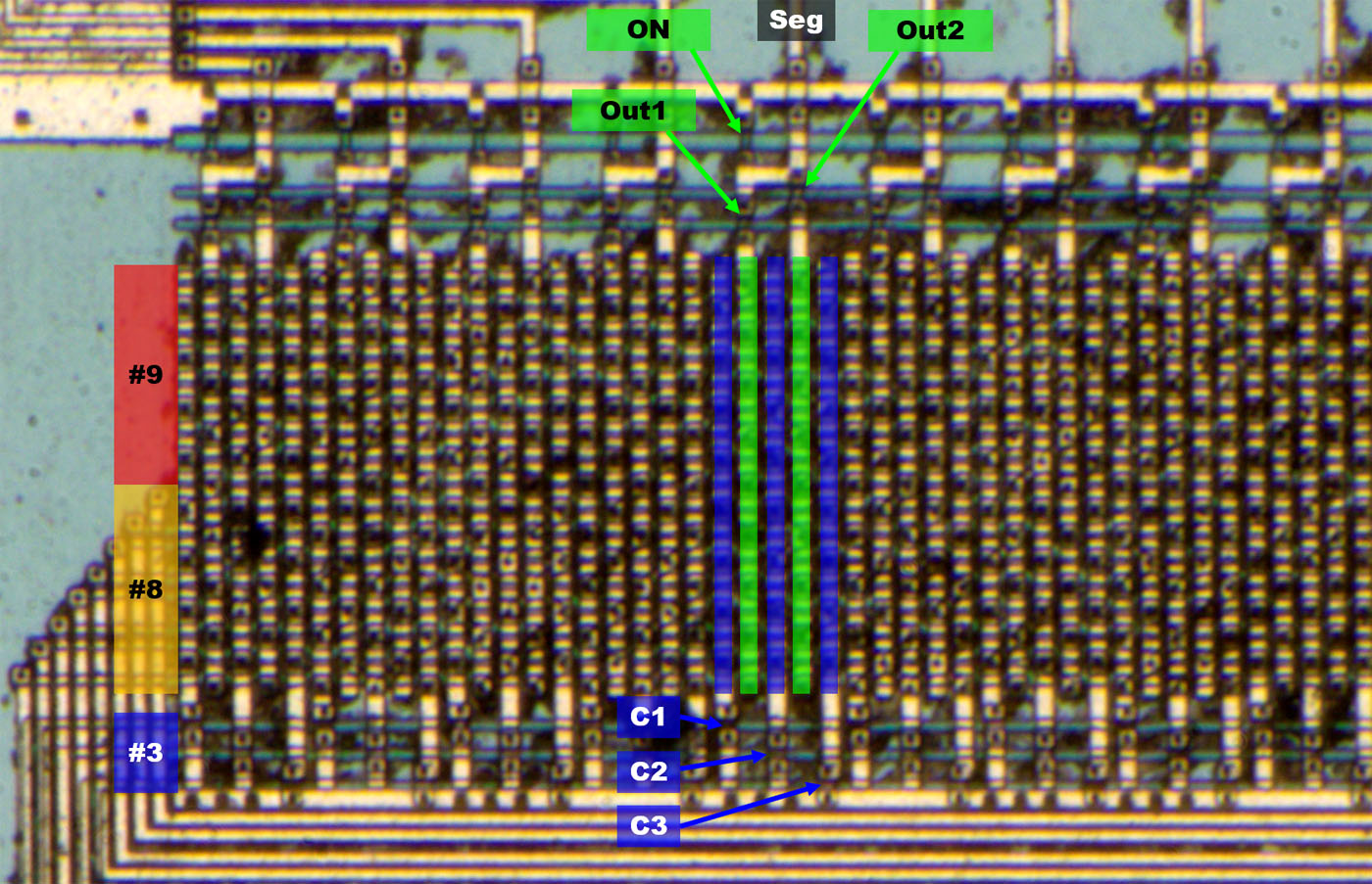
From left and right there are 8 and 9 control lines (yellow/red). But that would give us just a 17x17 ROM, not enough for the character set.
On the upper edge you can spot three transistors. One transistor (ON) allows us to switch every segment on, probably for a cursor functionality. Two transistors (OUT1/OUT2) switch the segment driver to one of two vertical lines (green). That expands the memory to 17x17x2 or 17x34, still not enough.
There are three more control lines below the memory array (blue). These control lines switch three transistors (C1/C2/C3) that activate three vertical lines around the two green output lines. That expands the memory to 17x17x3 (17x51), still not enough in the first place. There has to be 12 characters which are generated by adding two other characters, i.e. by activating more than two vertical lines.
https://www.richis-lab.de/Opto10.htm 


