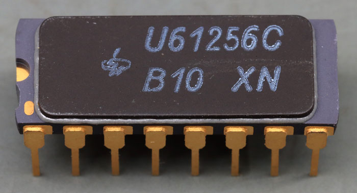
The 256kBit DRAM U61256 was developed at the Zentrum für Mikroelektronik in Dresden. It was the largest mass-produced RAM in the GDR. The subsequent 1MBit memory U61000 was only produced in a small series. The characters XN indicate production in November 1989.
The numbers 10 stand for the first selection type, which allowed access times of 100ns. This was followed by selection type 08, which was specified with 80ns. The basic type (12) offers access times of 120ns, the slowest bin (15) has an access time of 150ns.
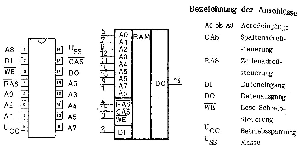
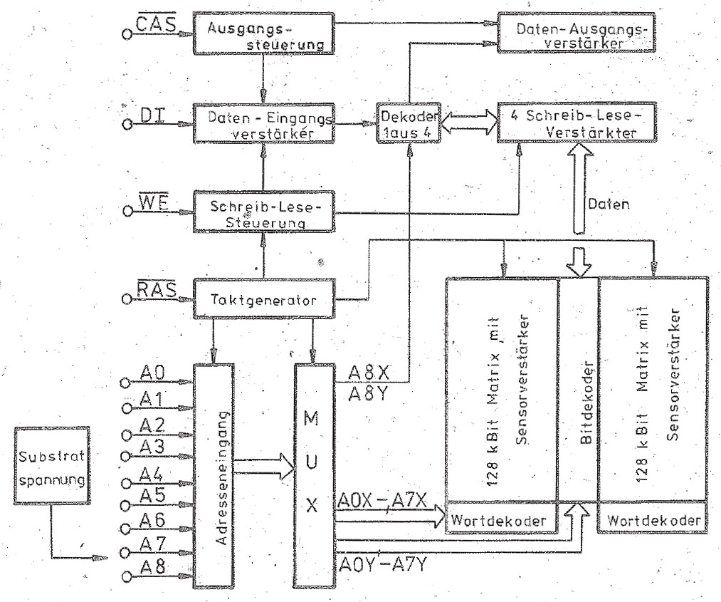
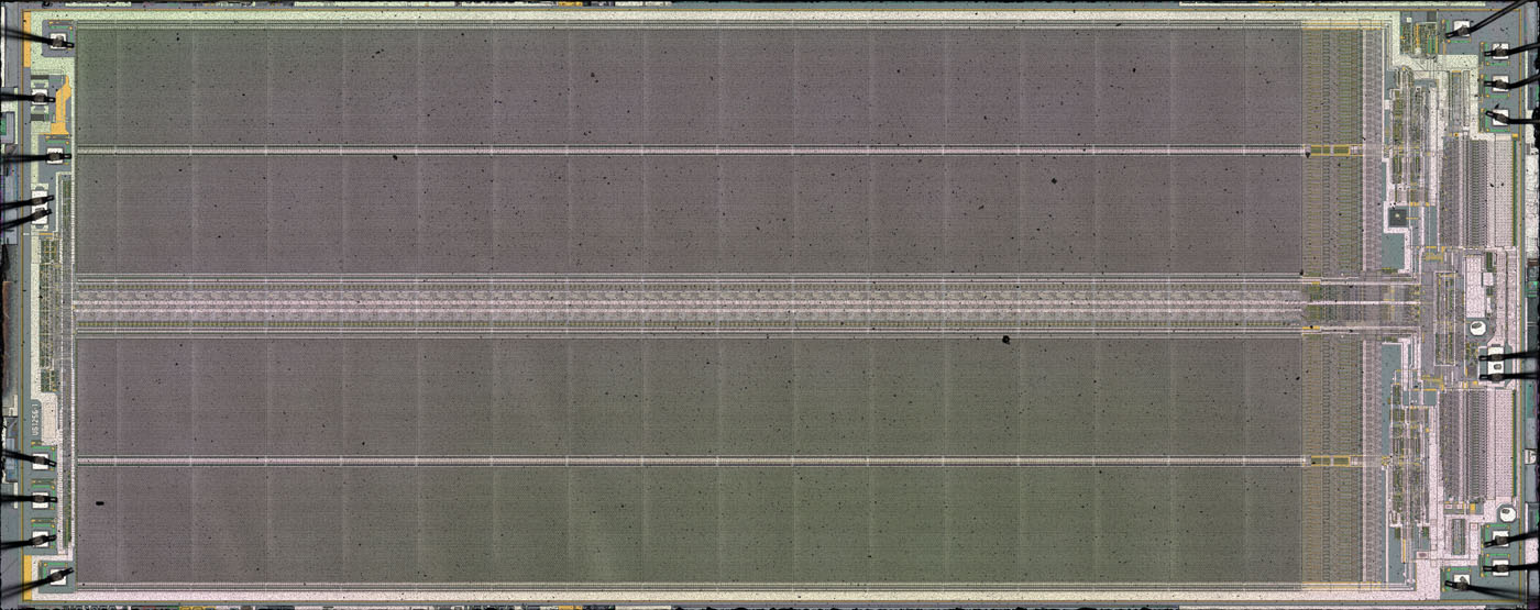
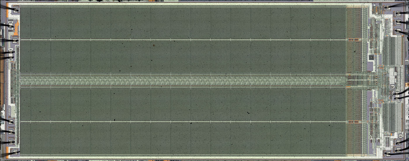
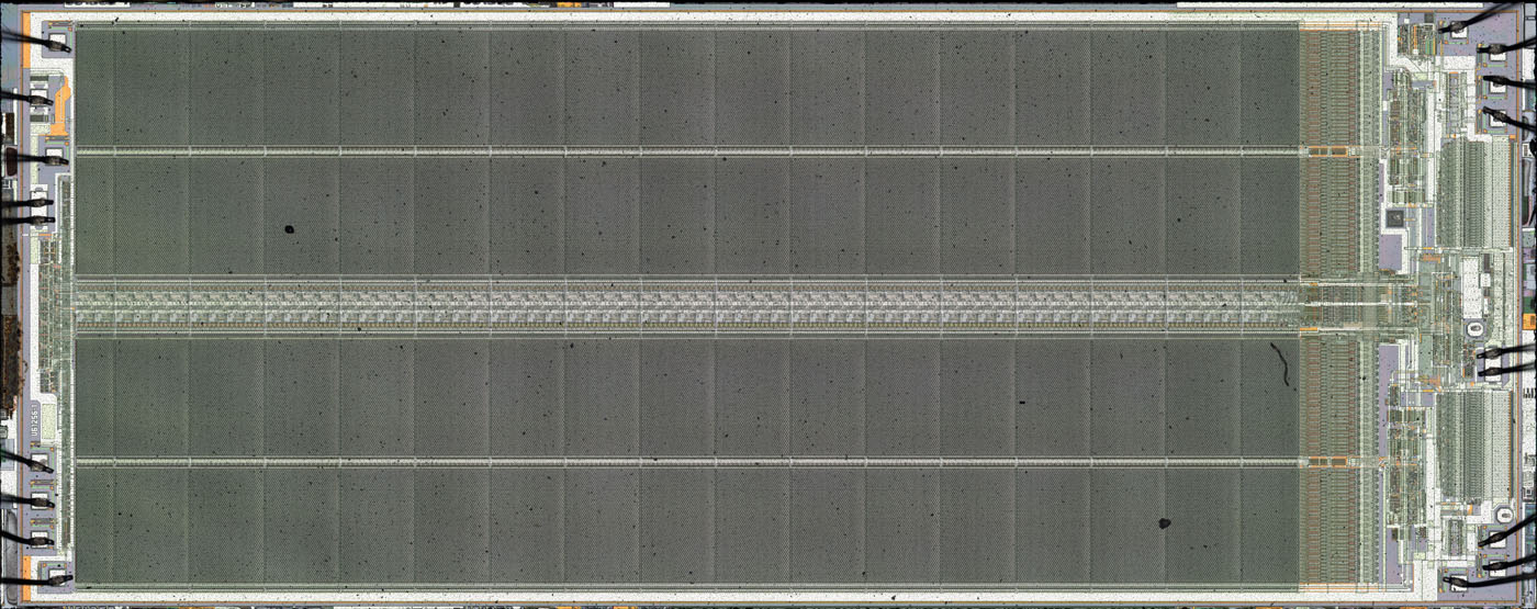
The datasheet shows the structure and function of the U61256. 8 bits of the 9-bit wide addressing interface are first decoded for row selection and then for column selection. The memory consists of two 128kBit areas which output the information of four cells simultaneously when reading data. The ninth bit of the addressing interface, which is also evaluated twice, controls the selection of one of these four cells. The data output in the top right-hand corner is missing in the block diagram.
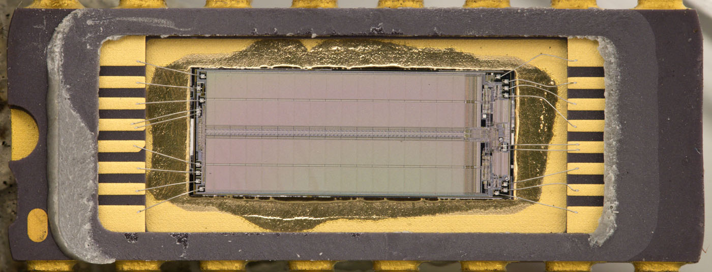
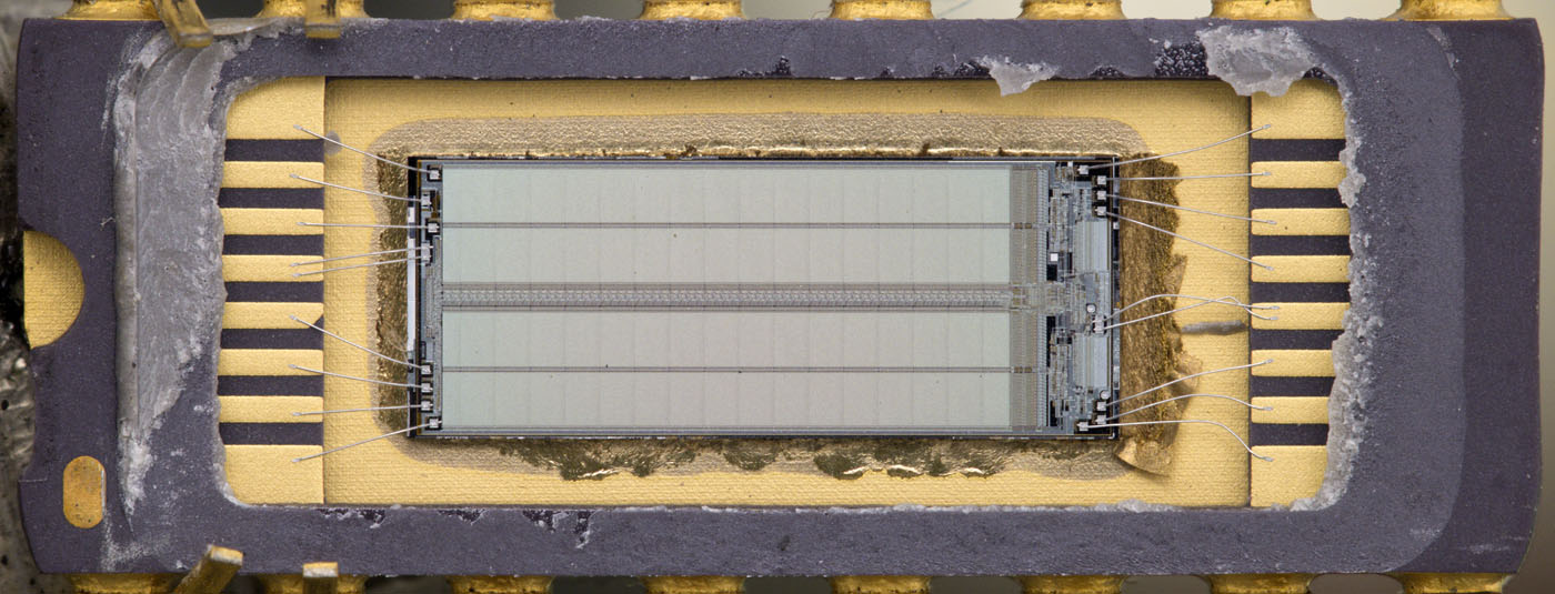
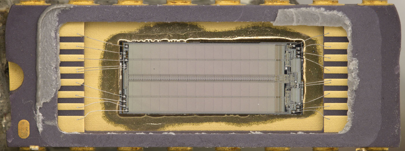
The size of the die is 9,6mm x 3,8mm. Each supply potentials is routed to the die with two bondwires.
The image of this is also available in a higher resolution:
https://www.richis-lab.de/images/RAM/10x03XL.jpg (67MB)
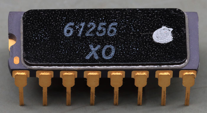
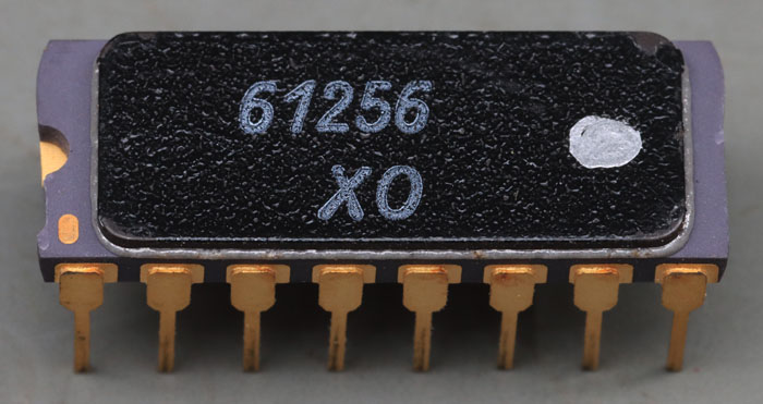
Here you can see another U61256. The bin marking is missing on this component. XO indicates production in October 1989.
The image of this part is also available in a higher resolution:
https://www.richis-lab.de/images/RAM/11x03XL.jpg (71MB)
The third U61256 appears to come from the same batch as the second.
The image of this part is also available in a higher resolution:
https://www.richis-lab.de/images/RAM/12x03XL.jpg (71MB)
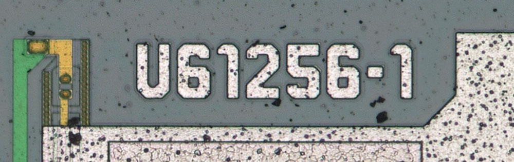
All three dies are labelled U61256-1. The number 1 probably indicates the first revision of the design. Fittingly, I can´t see a difference in the three parts.
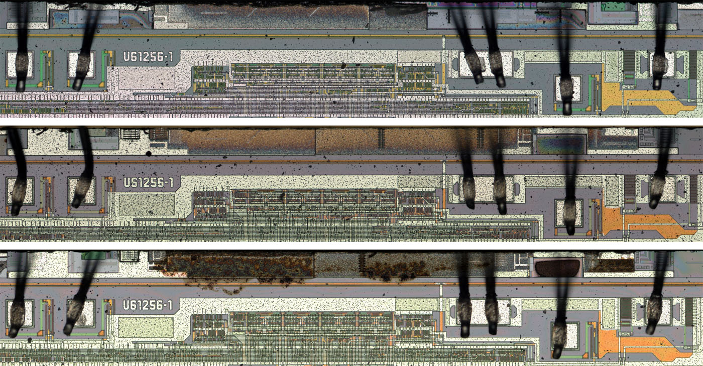
The left-hand edge appears to have had some imperfections during production. The third part shows soiling or signs of corrosion that extend to the first active structures.

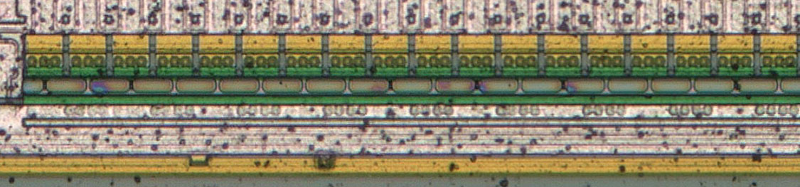
On the upper edge you can see some masks.
The metal layer appears to have penetrated from the contacts into the polysilicon layer in many areas. The effect can be found in all three parts. The section shown here is from the third part.
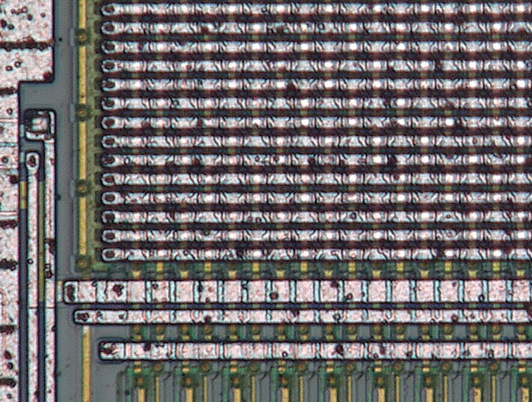
The memory cells are too small and there are too many layers on top of each other to be able to clearly recognise the structure. The surface structure of the metal layer appears to show capacitor geometries similar to those in the U2164.
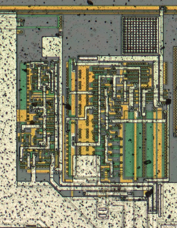
As in the U2164, line selection in the U61256 also takes place laterally and data evaluation is placed at the lower or upper edge of the storage areas. In contrast to the U2164, however, the lines in the metal layer run horizontally rather than vertically.
The memory area only has line drivers on the right-hand side. Correspondingly large driver transistors are integrated there in order to be able to represent the necessary charging current. This could also be an explanation for the horizontal lines in the metal layer. The metal layer has a lower impedance than the polysilicon layer.
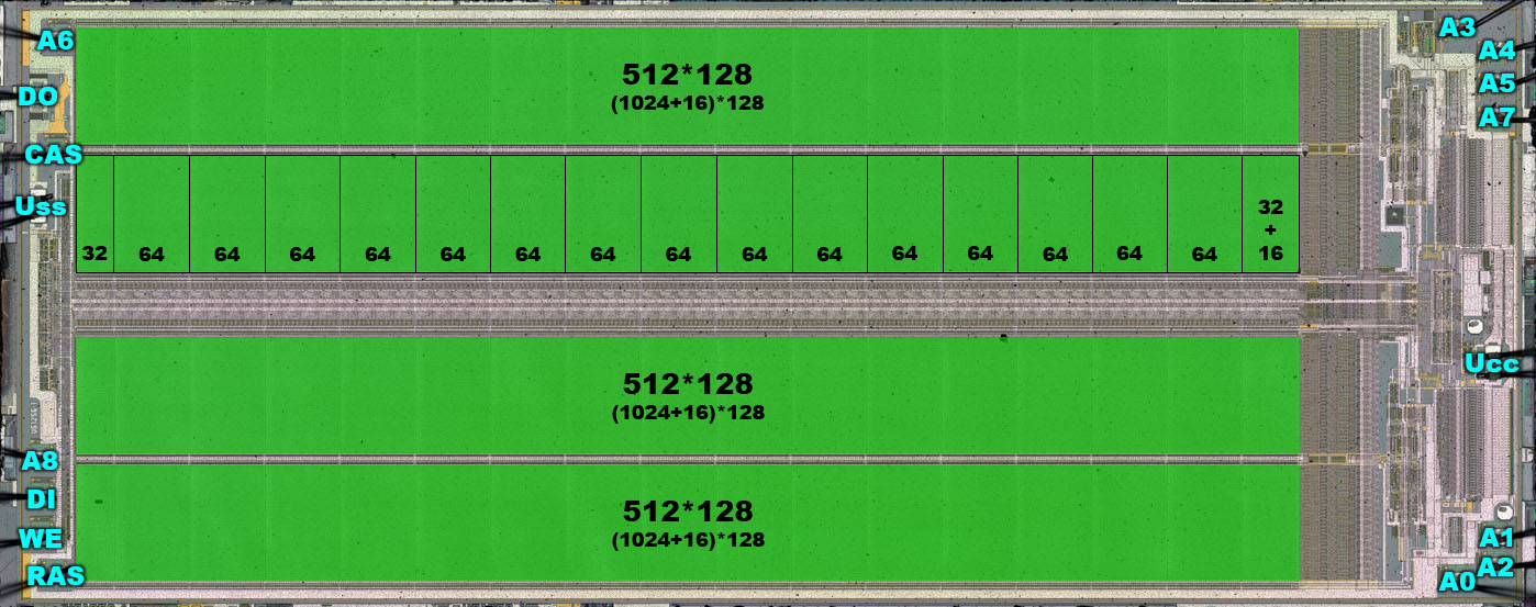
In the block diagram, the memory area is divided into two parts. The upper and lower blocks each consist of two areas. Each of these areas contains 15 segments, from each of which 64 lines lead out of the area. There are 32 lines at the beginning and 32 at the end. This results in a total of 256.000 memory cells. There are 16 additional columns on the right-hand edge. Apparently, the memory has 16 reserve columns, i.e. 8.192 additional memory cells, to compensate for production errors.
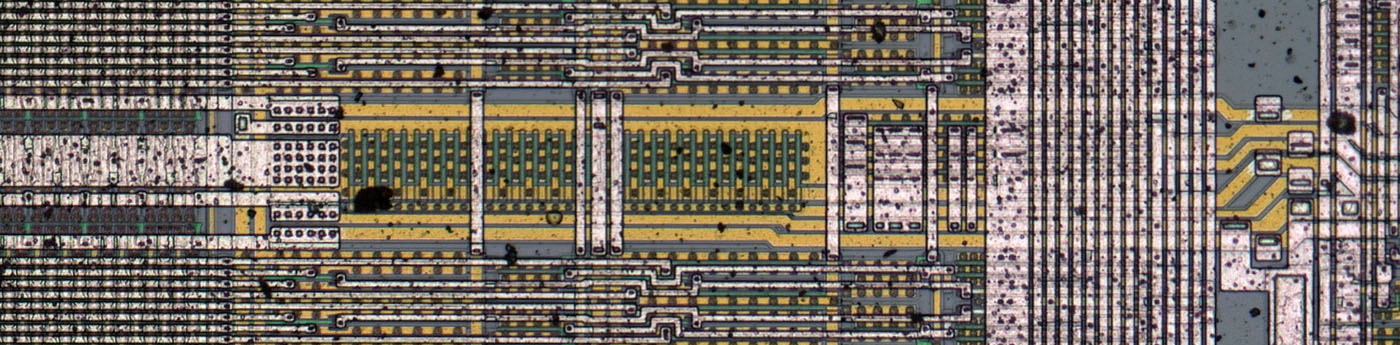
Here you can see the structures that run through the two large storage areas. The supply lines are relatively massive. Perhaps they are used to preload the columns before the memory cells are read.
Even if the exact structures of the column selection cannot be recognised, some functions can be surmised. Two times eight lines run horizontally between the two large memory blocks. These are most probably the address lines for the two memory blocks. Four lines run somewhat shielded from this in the centre, which then certainly transmit the four memory contents readout.
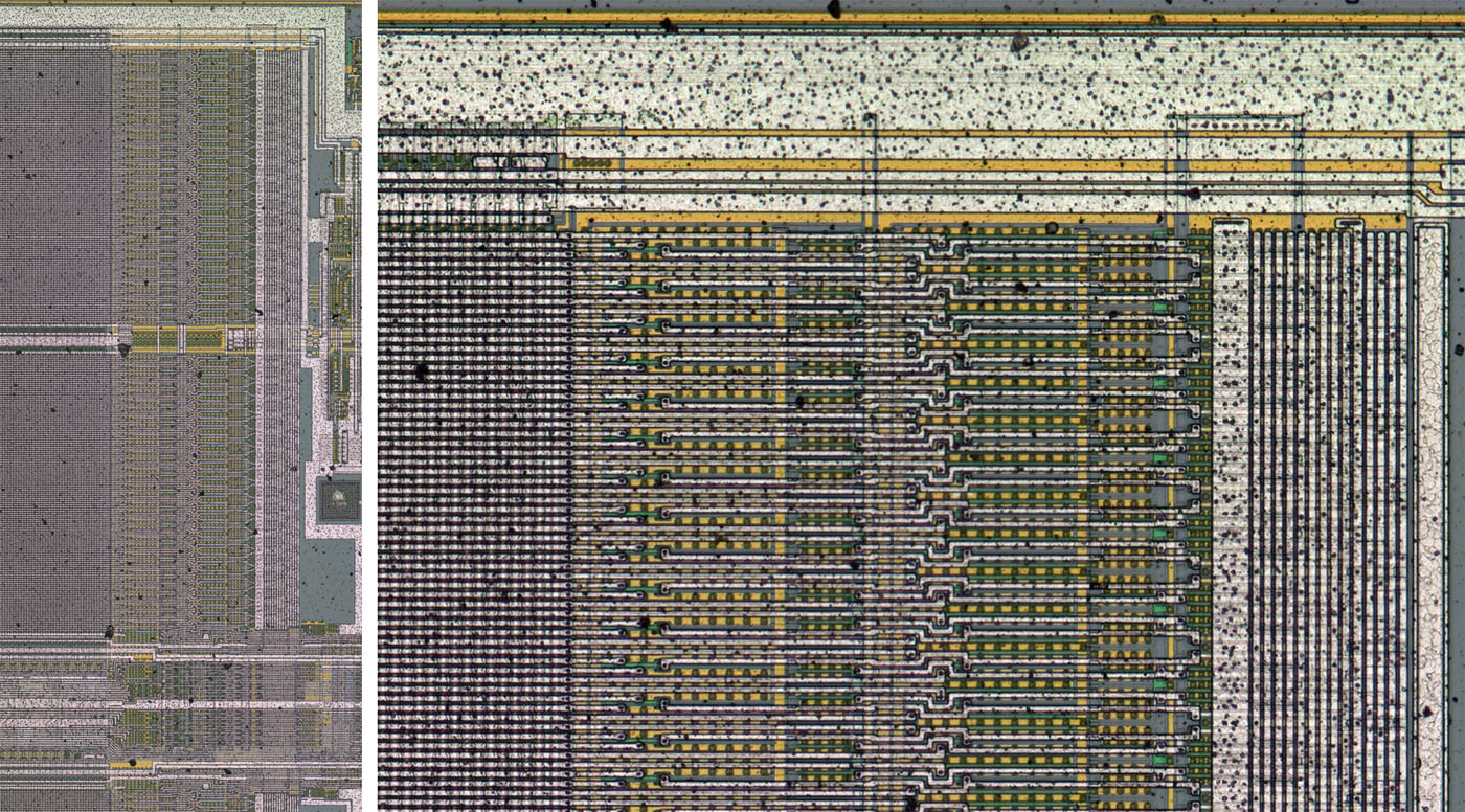
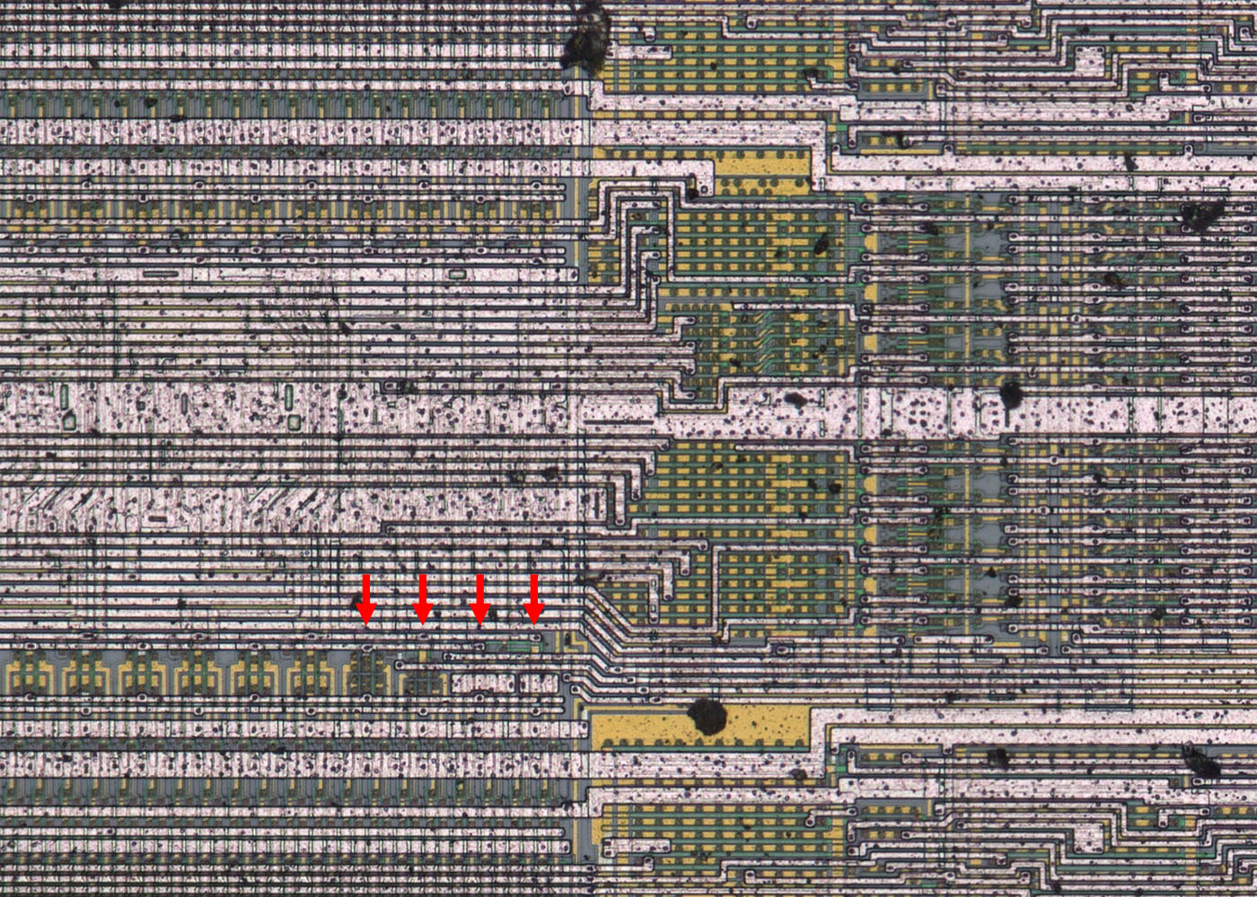
The fact that the 16 columns on the right are the reserve columns can also be seen here (red arrows). The first four blocks, which read out four columns each, are constructed and contacted differently. Five additional control lines are routed to this area.
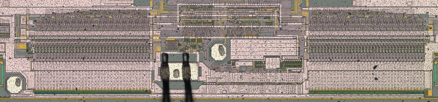
The circuit that enables the reserve columns to be looped into the address range is integrated on the right-hand edge. There are two times 36 fuses near the edge of the die for this purpose. The triggering is apparently similar to that of the U2164. Two testpads are integrated, one of which transmits the triggering current.
The triggered fuses can be easily recognised. The fuses are thin polysilicon strips. Some fuses were triggered in all three parts. Apparently there were defective cells in all three parts.
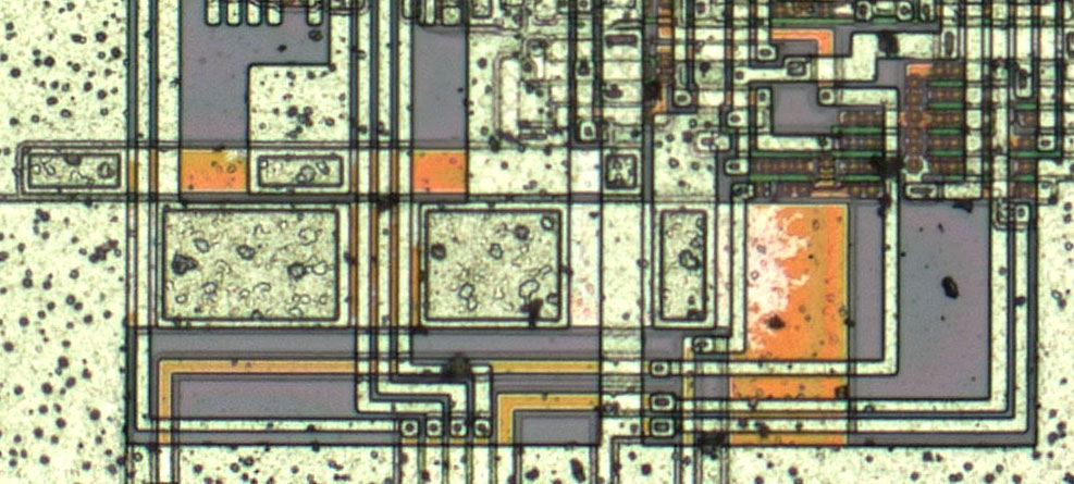
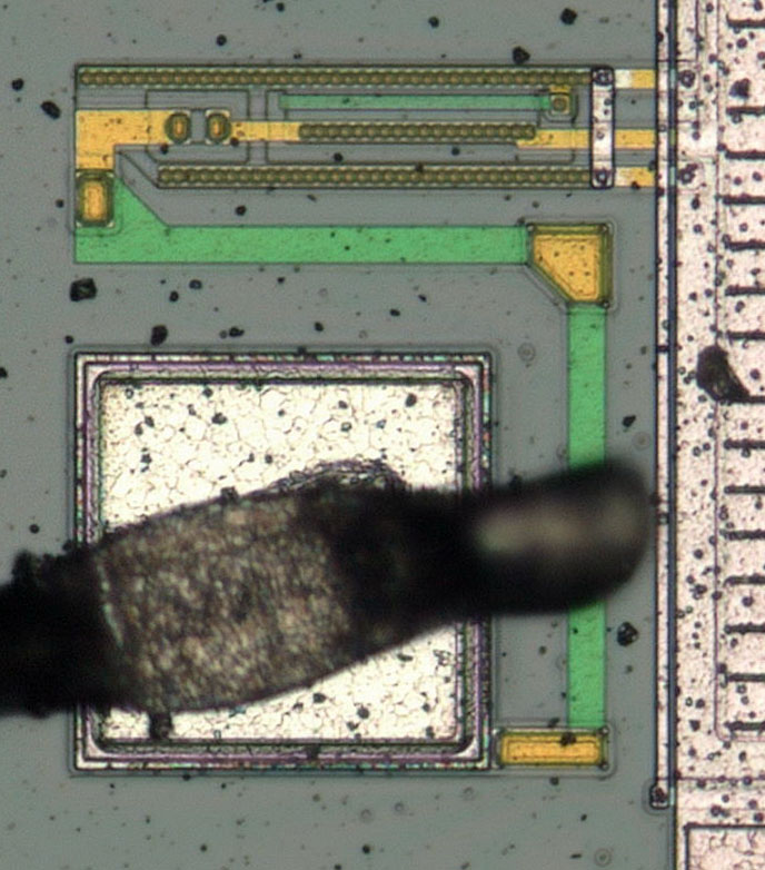
The bias voltage generation is located in the top right-hand corner of the die, which places the substrate at a negative potential. In the upper area, the circuit contacts the frame structure. This potential is also used in some parts of the circuit.
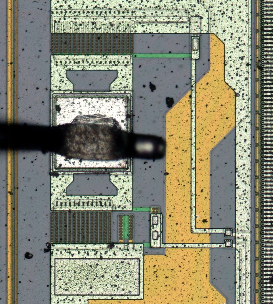
In addition to the two testpads for triggering the fuses, there are two further testpads on the die. It is interesting to note that the surface of these testpads has a different structure. It could be that two types of testpads were used depending on the application. The testpads of the fuses are always contacted during production. The bias voltage probably only rarely needs to be measured. This testpad is also significantly smaller. The function of the fourth testpad remains unclear. Although its surface is structured in the same way as the bias voltage generation testpad, it was contacted for all three components.
Here you can see an input protection circuit. It probably works in a similar way to the input protection circuit in the U2164. The two long, green elements are resistors for current limitation. In the upper area, two elements are surrounded by strips that are connected to the ground potential. The first element is probably a diode. The second element is a grounded gate NMOS.
The push-pull output stage of the data output is very easy to recognise.
https://www.richis-lab.de/RAM09.htm 


