I don't have much to input about any of the work you are doing because it is far beyond my scope of understanding, but I have to say, great work! It is really quite inspiring.
Hey, thanks, no worries.
---------------------------------------------------
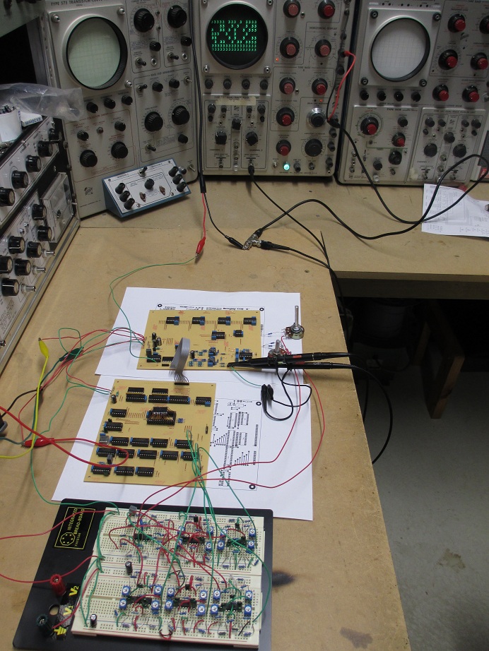
Here is the Fourier synthesis character display generator at its current level of completion. There will be 4 boards in total when finished. I have yet to etch and load the Fourier coefficient character ROM board and the sine/cosine filter board. The Sine/Cosine filters are currently (still) assembled on breadboard. There is no complete character ROM at the moment, just, for initial testing/running purposes, a single TL074 op-amp and several coefficient resistors assembled on the breadboard next to the filters to act as a single character ROM for the number 3.
The SOIC chip in the center of the board in the middle, sitting in the air on a piggyback DIP socket, is the SRAM which serves as the user-programmable screen RAM for the generated display. The SOIC is only temporary as I have a DIL-packaged version of the chip still to arrive on back order, which will substitute the SOIC. The part # is CY62256.
I ended up simplifying the remote programming logic by expanding the data bus to 12 bits. The programming of a specific character on the display is now just a simple matter of placing the 7-bit address value and the 5-bit character code (not ASCII) simultaneously on the 12-bit data bus and then strobing the programming port "write" control pin. This writes the address and character code data values in to a pair of latches (74HCT573) and the control logic automatically writes these to the screen RAM during the subsequent video blanking interval.
Each new character is drawn out on the CRT at 50uS intervals, 12.5uS of which is a blanking interval during which the CRT beam is cut-off. During this 12.5uS blanking interval the "write" control input to the programming port is disabled so that the latches cannot interrupted, and the screen RAM is written with the data stored in the larches. All this means that the screen RAM is programmed and updated without any interruption to the visible display.
However because the programming port is disabled during each 12.5uS blanking interval, and remote programming is completely asynchronous, the "write" control input of the remote programming port must be strobed for absolute minimum of 12.5uS plus a setup and hold time adequate for the latches to receive and store their data. So long as this simple requirement is met, the latches will be reliably written even if the rising edge of a "write" strobe on the programming port is time coincident with the very start of a blanking interval. This was about the simplest manner in which I could implement the remote programming logic.
All inputs to the remote programming port are TTL level compatible. Despite needing voltage level translation, the simple 12-bit port will make the display unit also directly compatible with the PDP8 work-alike digital computer project that I intend to start on once this analog computer is completed and out of the way.
The other assembled PCB contains the analog circuitry for generating the deflection circuitry. This includes a 2-channel by 16-way analog multiplexer, addressed by the data port of the screen RAM, which serves as the ROM multiplexer to select the character to displayed at any given position on the screen. The inputs to the multiplexer are currently not wired as I haven't assembled the ROM board yet. At the moment the only character that can be displayed is either a 3 or a blank space (as shown in the picture on on the scope CRT).
Dunno if all that babble makes the operation of the whole thing generally clear or not.