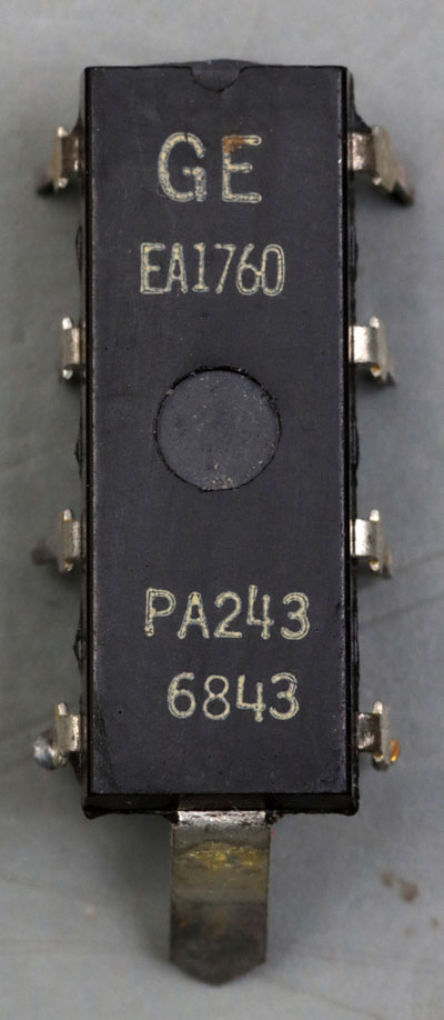
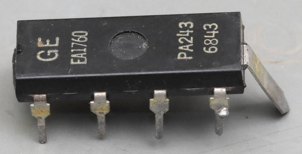
The PA243 is an audio amplifier built by General Electric. The date code refers to the year 1968. The most striking feature is the housing, which is based on a DIP-14 but has far fewer pins. Similar to Sanyo's LA4102 (
https://www.richis-lab.de/audioamp02.htm) a relatively wide metal strip improves heat dissipation from the interior.
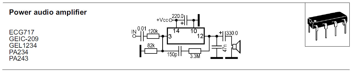
There is no datasheet for the PA243. In the "Audio Amplifiers Databook" at least an example circuit is shown and comparison types are mentioned: ECG717, GEIC-209, GEL1234 and PA234.
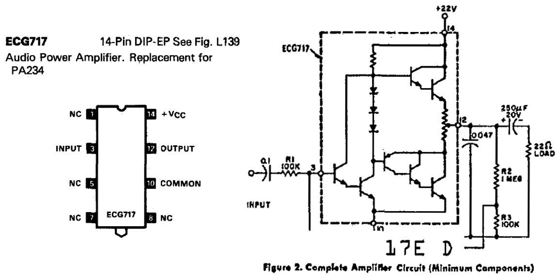
For the ECG717 a datasheet can be found. According to this, the supply voltage must be between 9V and 25V. The quiescent current is between 1mA and 15mA. The load impedance must not drop below 8Ω and is specified up to 22Ω, where 22Ω is the typical value. The output impedance is specified as 2Ω. The bandwidth is 30Hz - 100kHz (at 0,5W output power).
At 22V, the datasheet guarantees a minimum output power of 1W (3% THD typical, 10% THD maximum). Due to the low efficiency of 46% (22V, 22Ω, 1W) one has to pay attention to sufficient heat dissipation. If the heat sink of the component is kept at 50°C, up to 1,4W of power loss can be dissipated. Without this heatsink, just 0,8W is permissible even at 25°C.
The datasheet shows an example circuit too. Due to the simple supply, coupling capacitors are necessary at the input as well as at the output. The output signal is fed back via the voltage divider R2/R3. The value of the resistor R1 varies the amplification factor (2,4 - 47). The capacitor directly at the output provides the necessary high-frequency stability. The datasheet points out that this rather simple measure significantly increases the current consumption of the amplifier for signals above 15kHz.
The integrated circuit has two transistors at the input, which are an unusual Darlington pair. The collector connection of the first transistor is not directly connected to the collector of the second transistor. Between the two collectors are the three diodes, which create a certain voltage drop and thus a bias current through the output stage.
The input amplifier is immediately followed by the quasi-complementary output stage. The highside transistor consists of a Darlington circuit. On the lowside there is a Sziklay circuit, which also contains a Darlington pair inside. The PNP transistor just provides the necessary phase inversion, the current amplification is realised by the two NPN transistors.
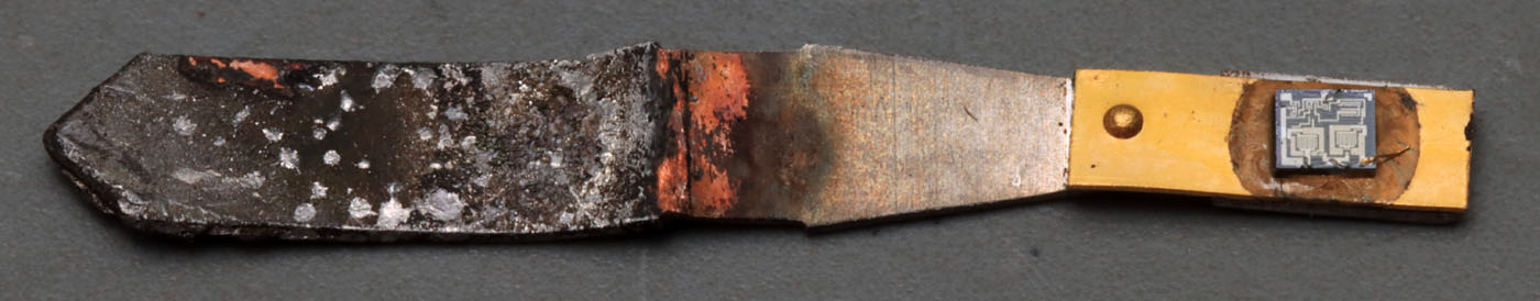
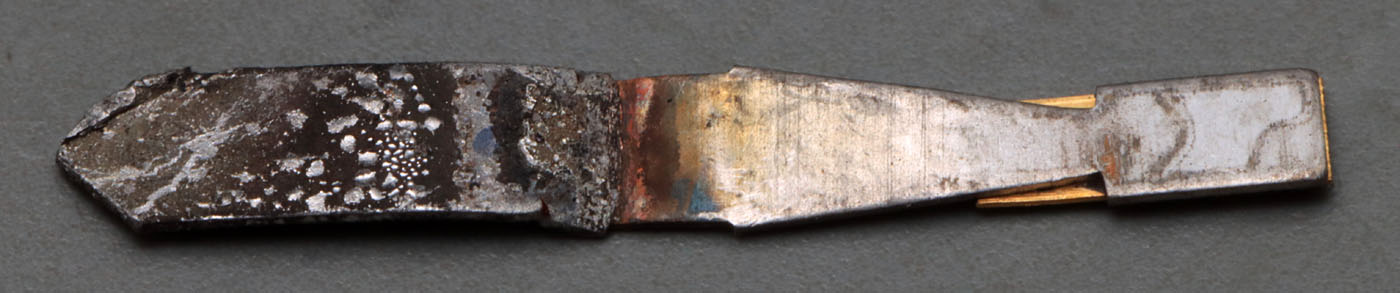
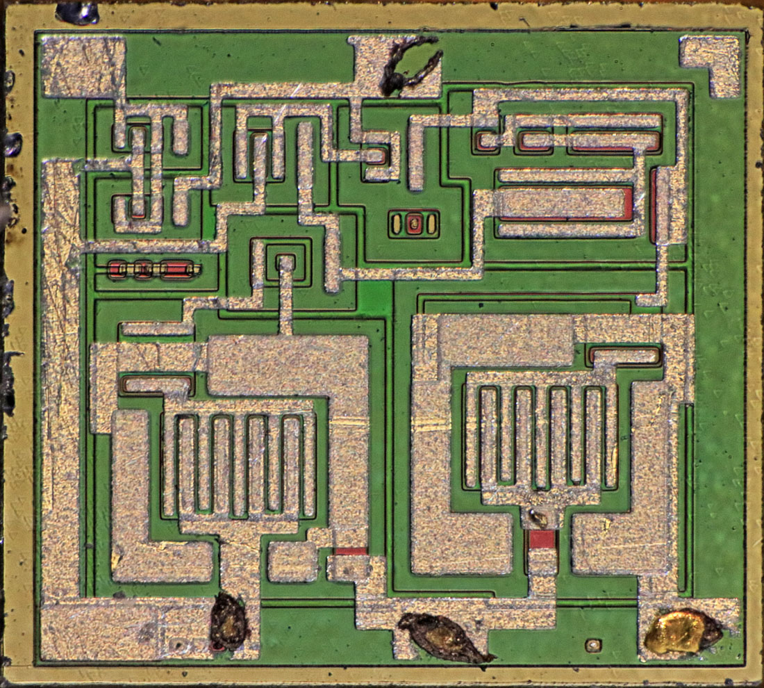
If one removes the housing material, it becomes apparent that a gold-plated element is applied to the cooling fin, on which the die is located. From a thermal resistance point of view, the additional element is not optimal. Perhaps this design facilitated the manufacture or the different coefficients of thermal expansion made the additional element necessary.
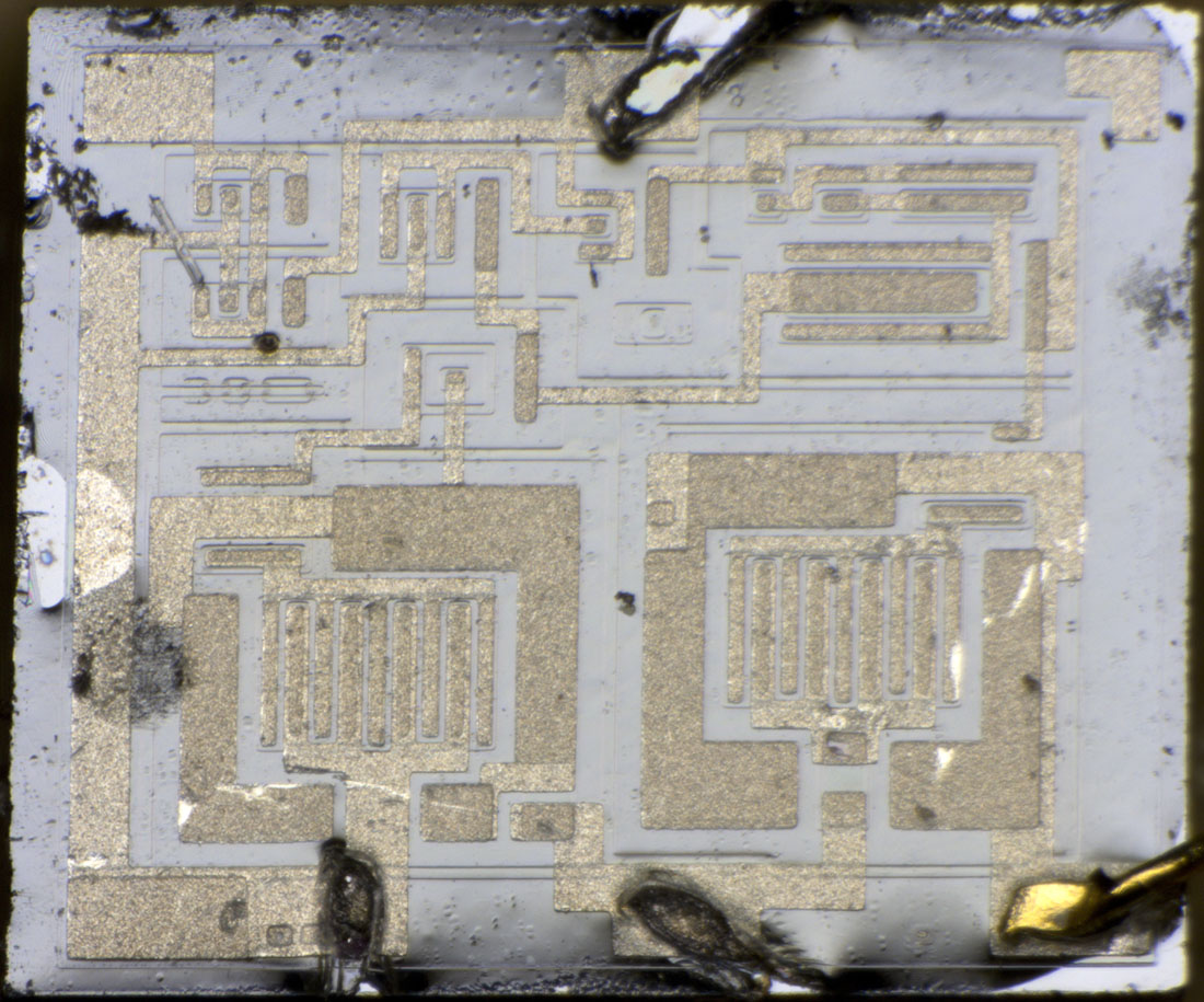
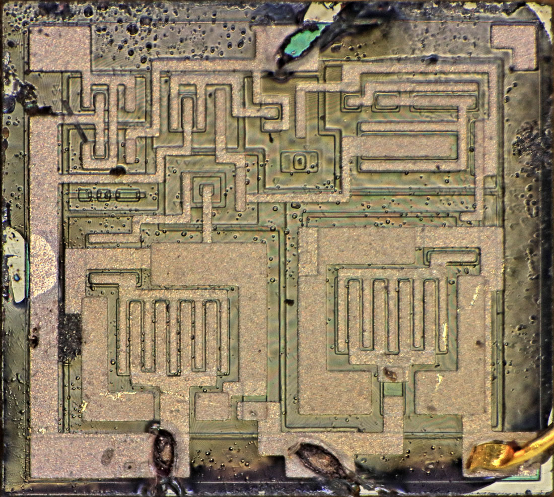
The dimensions of the die are 1,3 x 1,2mm. It is covered with a transparent but not completely clear protective layer.
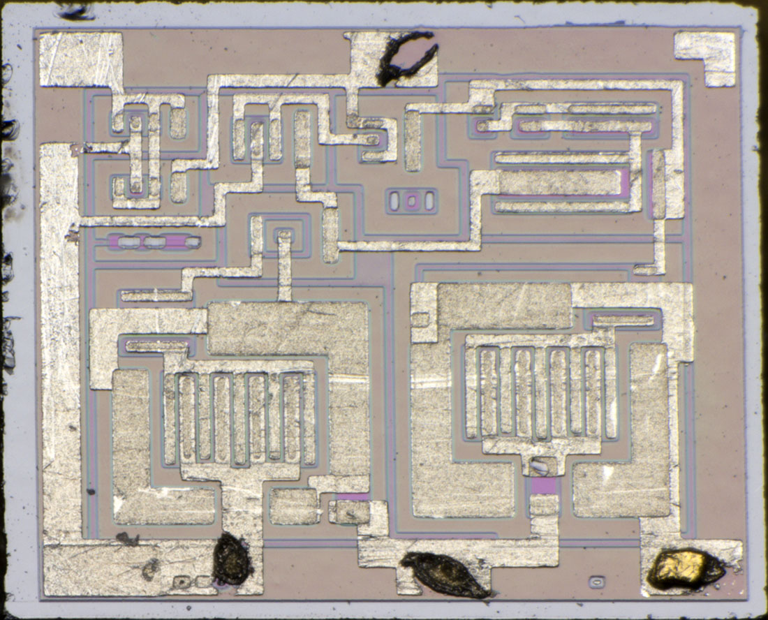
The protective layer remains stable even after a longer dwell time in a paint stripper. Only a longer dwell time in a silicone remover ultimately leads to the coating being able to be rubbed off. The structures are hardly damaged in the process. However, it turns out that the metal layer is not protected by a passivation layer. The removal of the coating resulted in scratches and minor damage in several places.
There are some irregularly distributed triangular contours on the surface of the die. These could be an artefact of an etching process.
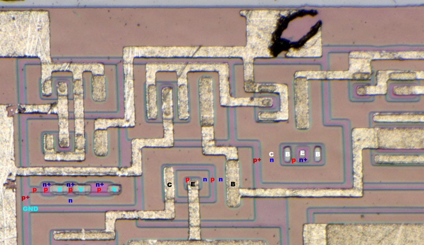
The individual elements can easily be identified. A NPN transistor, which has not been contacted, is integrated in the input area. It is located in a common n-doped collector area with the input transistor. A buried collector is not visible. Either the conductivity of the n-doping is sufficient or the buried collector do not stand out visually. The n-doped surfaces are surrounded by heavily p-doped insulation frames. A p-doped base area with two contacts is inserted into the collector surface. This base area in turn contains the heavily n-doped emitter area with the corresponding via.
A PNP transistor is integrated to the left of the NPN transistor. This is the classic, lateral construction. The p-doping, which is otherwise used as base doping, represents the collector and emitter here. The n-doping, which is otherwise used as a collector, represents the base area here. The relatively large distances lead to the clearly worse values of a PNP transistor compared to the values of an NPN transistor.
On the left is an unused resistor. It is a pinch resistor where the base doping (p) represents the resistance, which is narrowed by a superimposed emitter doping (n+) so that the resistance value increases. On the far left, the resistor is connected to the insulation frame and thus to GND. These are three resistors connected in series, which could be contacted through three vias.
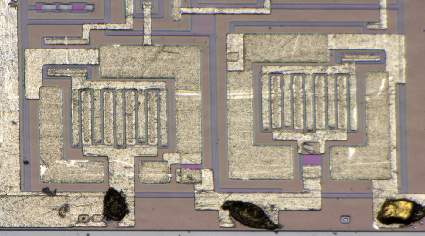
The two Darlington output stages are located in the lower area of the die. The driver transistor is integrated with the power transistor in the same collector area. The collector connection of the power transistor is massive over the whole circumference. This suggests that the collector connection is relatively inefficient. As already described, no contours of a buried collector can be seen. The base areas of the driver transistors are used to undercut the collector contacts.
The low-impedance resistors at the output consist of the heavily n-doped emitter material, which is located in base surfaces for insulation.
Several squares are integrated at the lower edge, allowing the alignment of the masks to be checked. One square is clearly visible in the right area, three more squares are located under the metal layer at the left bondpad.
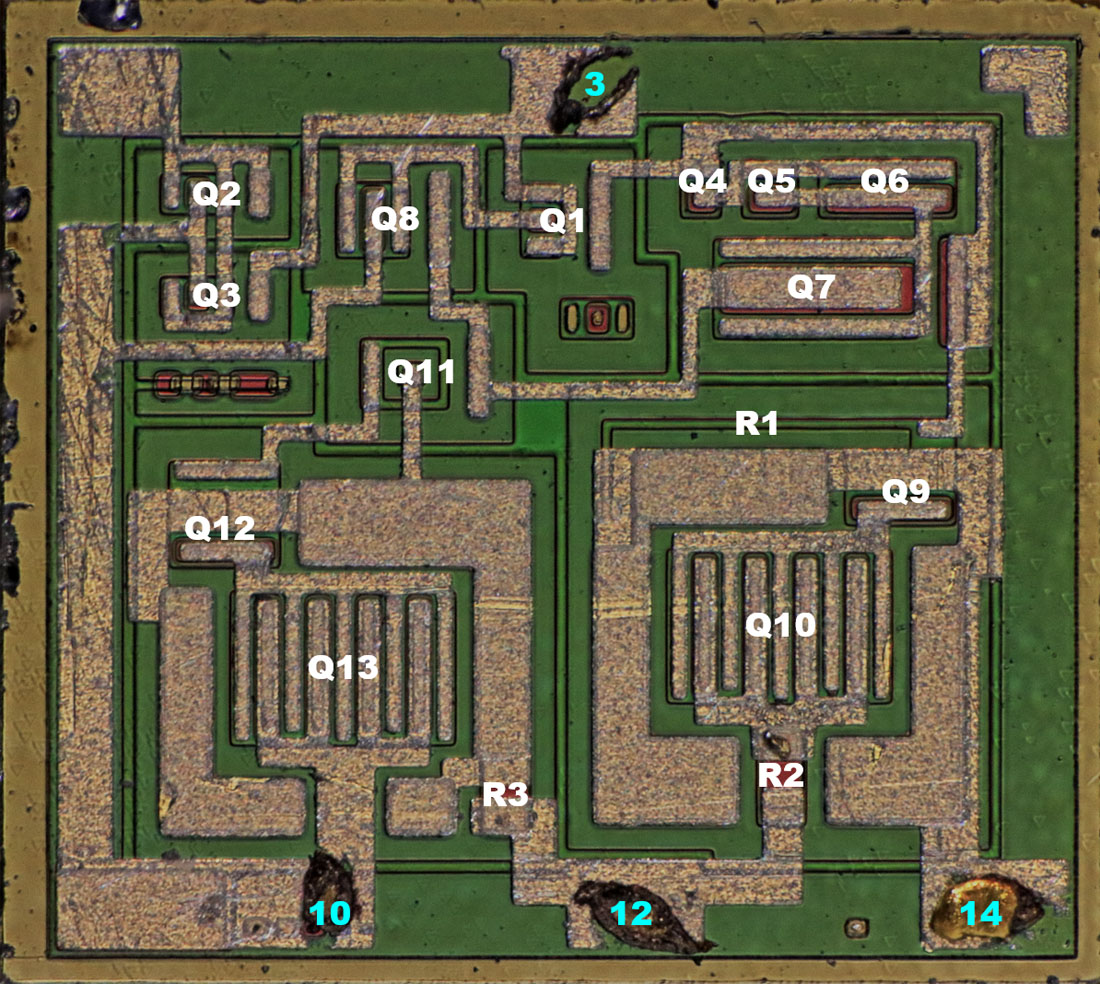
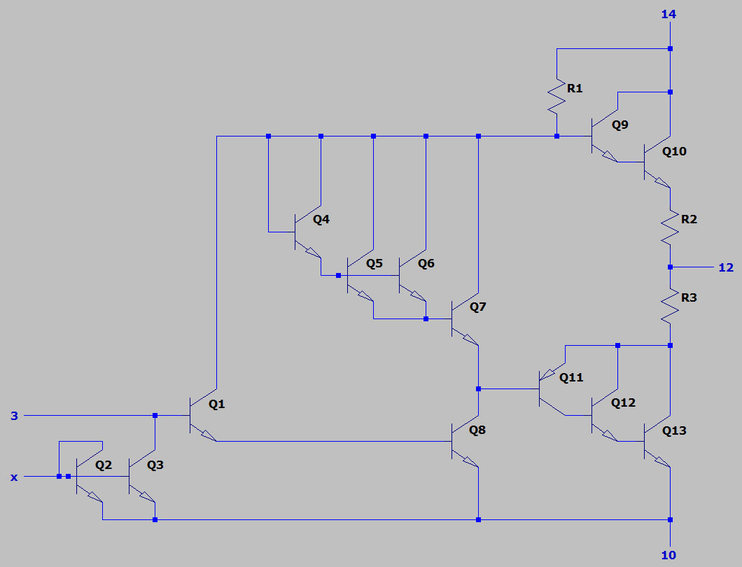
If we analyse the circuit, we see that it is broadly similar to the circuit shown in the datasheet of the ECG717. In the PA243 there is an unused bondpad connected to the two transistors Q2/Q3 at the input. This seems to be a disable circuit of the input.
The unused transistor in the collector area of the input transistor Q1 could be a hold-off to add a third transistor to the Darlington pair Q1/Q8 to further increase the gain.
The diodes for setting the bias current are represented by four transistors of different sizes (Q4-Q7). This way, you can adjust the voltage drop and thus the bias current with a variation of the metal layer.
https://www.richis-lab.de/audioamp06.htm 


