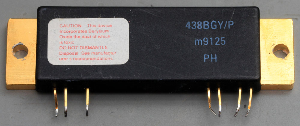
The Mullard 438BGY is an old RF amplifier (>18W between 68 and 88MHz).
First ad for the 438BGY was found 1974.
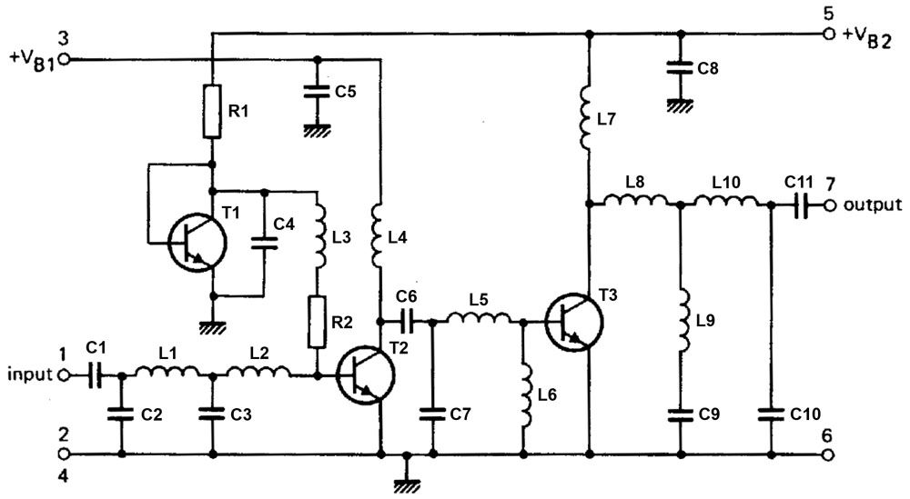
You don´t find much information about the 438BGY but the schematic of the BGY32, BGY33, BGY35 and BGY36 fits quite well. I added the part numbers, we will need them later.
There is a preamp around the transistor T2 and a output stage around T3. At the inputs and outputs there are some LCs for filtering and impedance matching.
T1 generates a bias so T2 doesn´t switch off completely. It´s interesting that T1 is supplied from the output stage (every stage has its own supply rail). I assume that supply concept should prevent oscillations because the phase shift is "better".
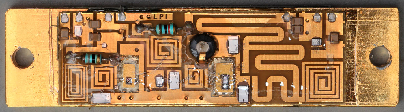
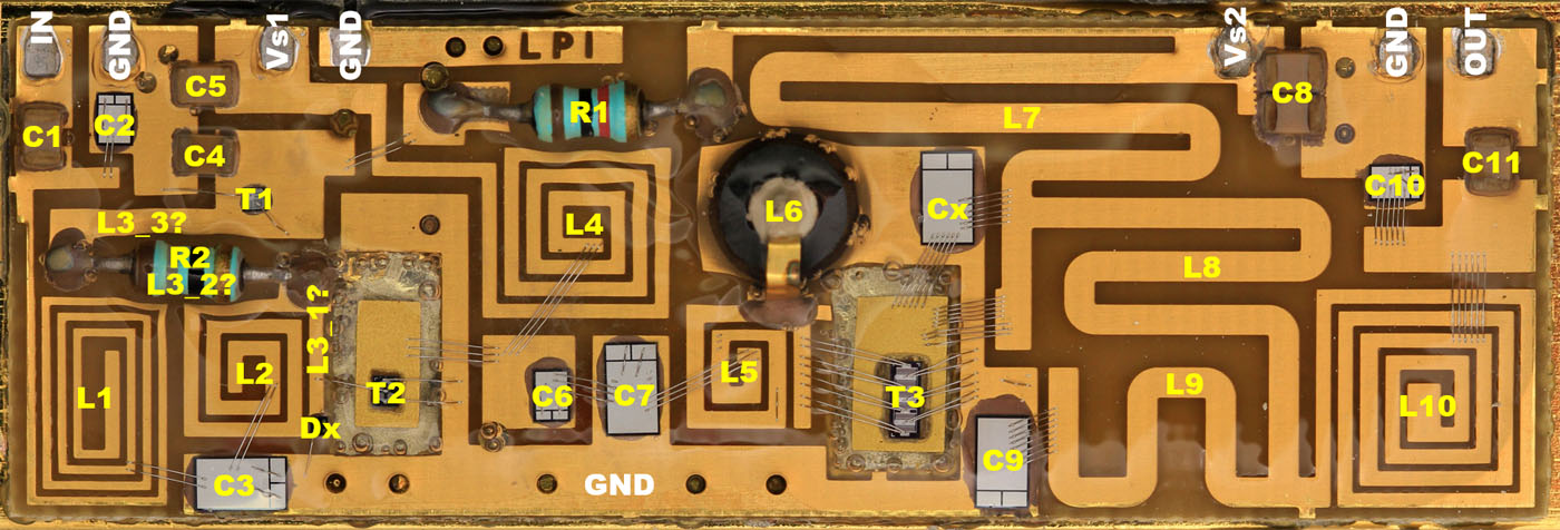
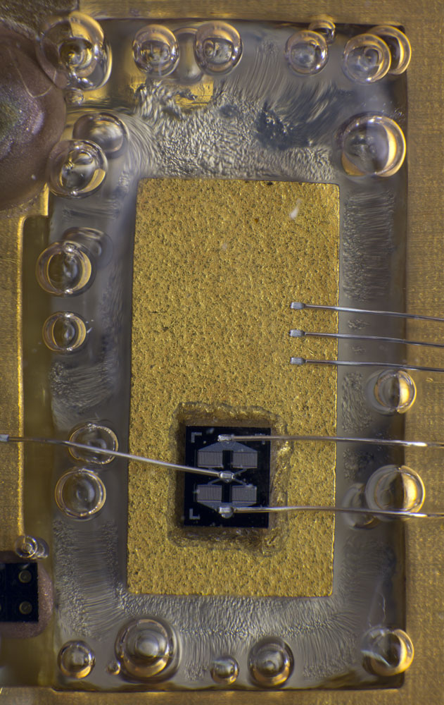
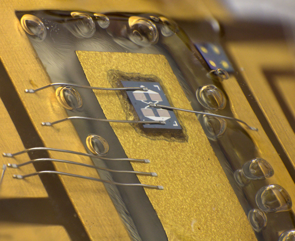
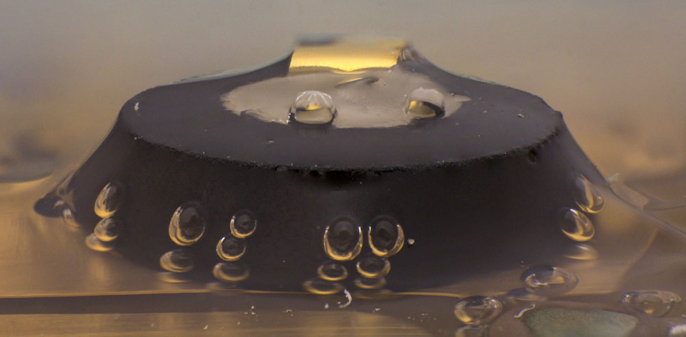
Removing the lid you find a PCB potted with some silicone gel. There are THT, SMT and bare die components.
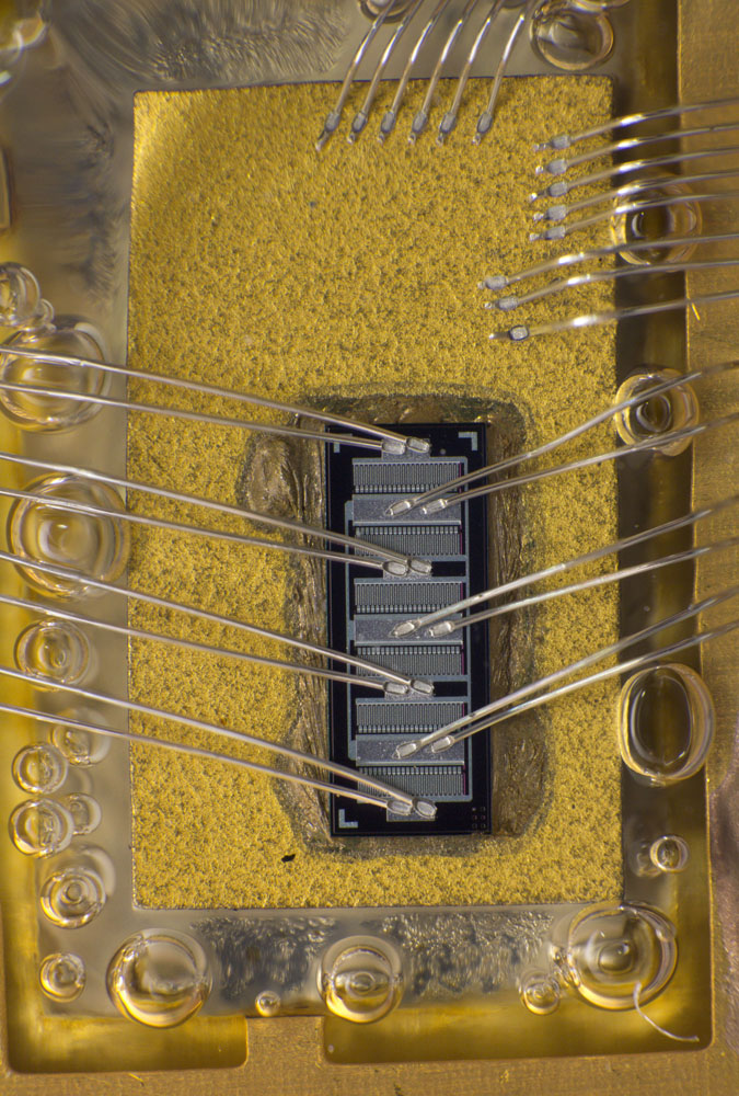
(Module turned around 180° so the signal flow is from left to right.)
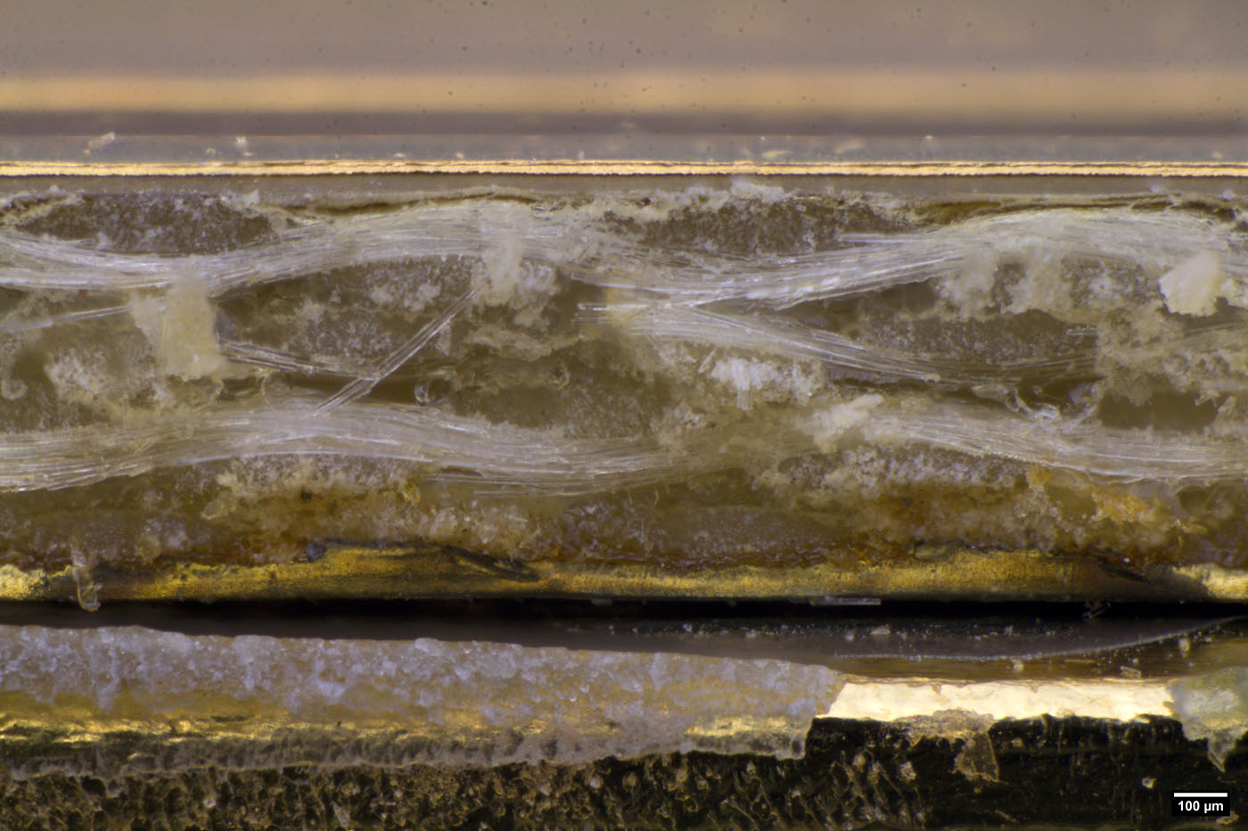
It´s a normal PCB with copper on both sides. You can see the glass fibre.
Vias are connecting the ground potential to the backside of the board. The heat sink acts as low impedance ground.
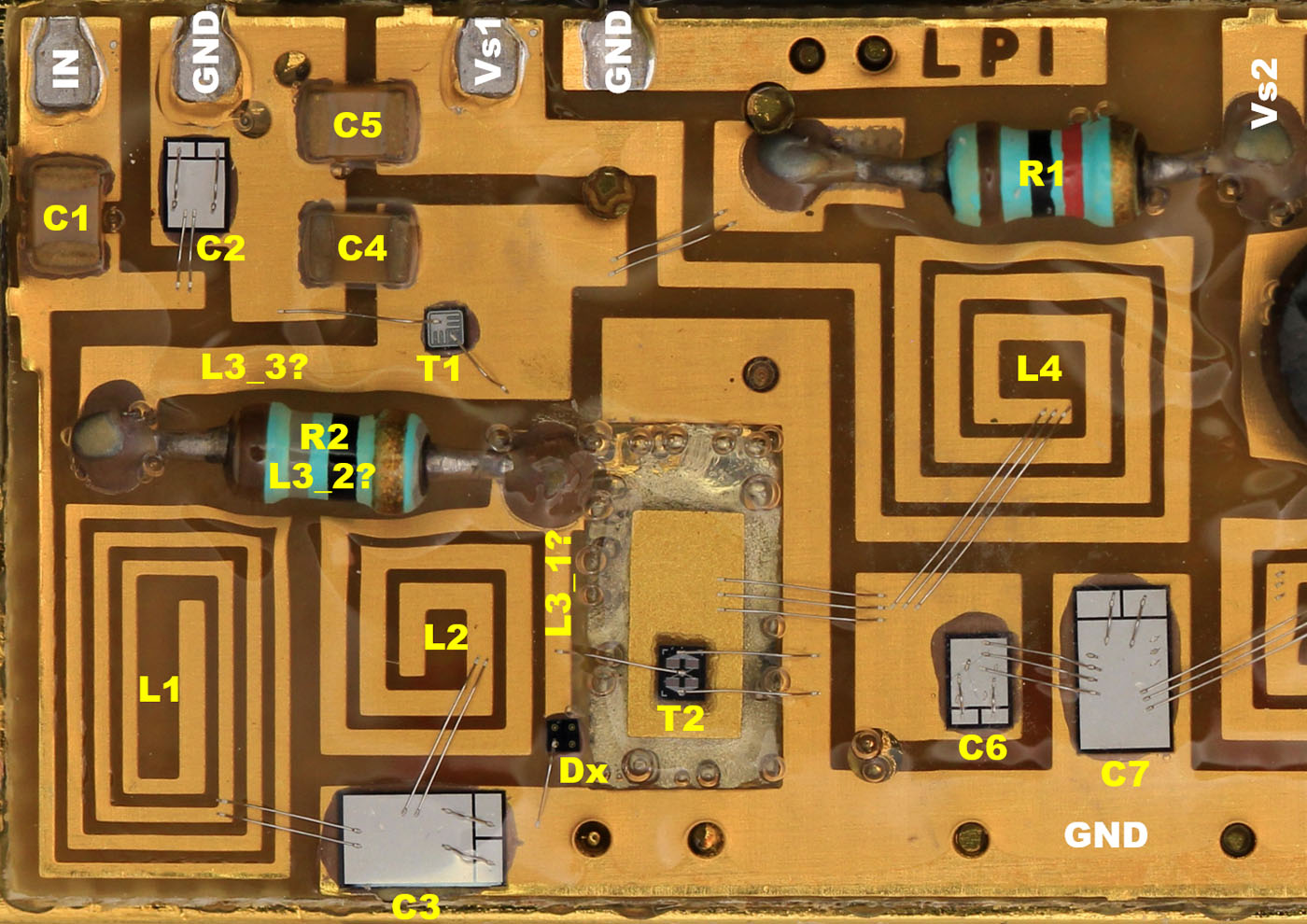
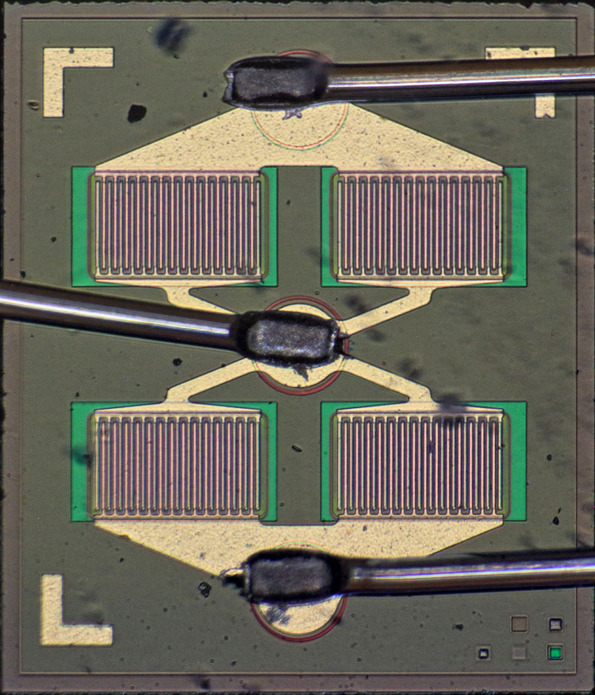
The preamp is on the left side. The only difference to the schematic is the diode Dx. The inductors are built with loops of copper on the PCB. It looks like the inductance L3 is distributed around the resistor R2.
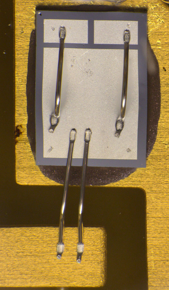
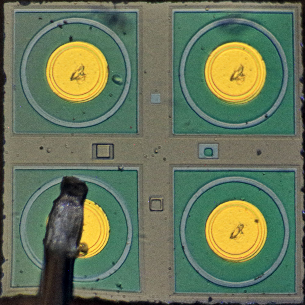
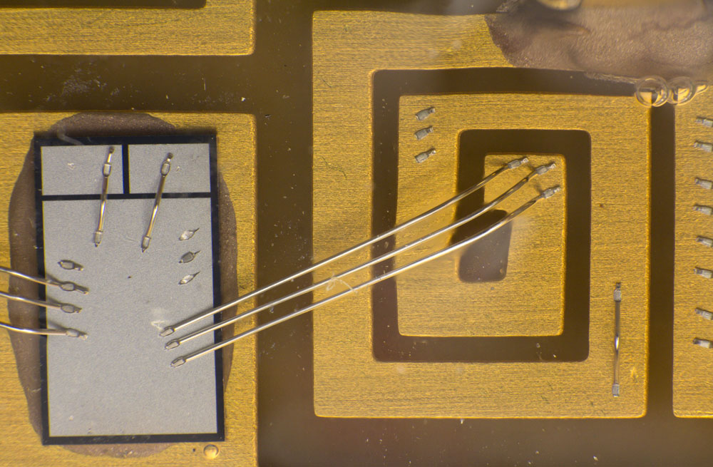
The smaller capacitors are built with silicon dies. There is a big and two small rectangles. You can adjust the capacitance by bonding the smaller areas to the main area.
T1 is a quite normal transistor since it just does the biasing.
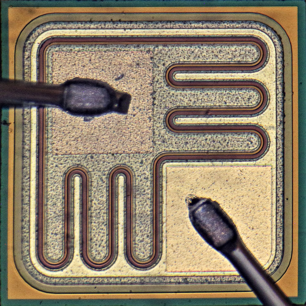
At the base of the preamp transistor T2 there is the diode Dx. It is integrated on a die with three other diodes. The diode protects the transistor against negative base emitter voltages.
The preamp transistor T2 is placed on a BeO ceramic. The BeO dissipates heat much faster than the PCB.
The preamp transistor T2 is a RF transistor with very thin emitter areas. Between the emitters there are the base contacts. A low base impedance allows fast switching.
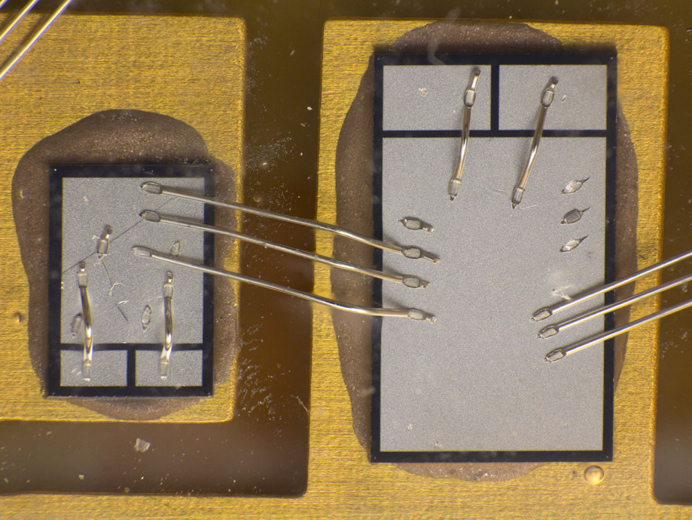
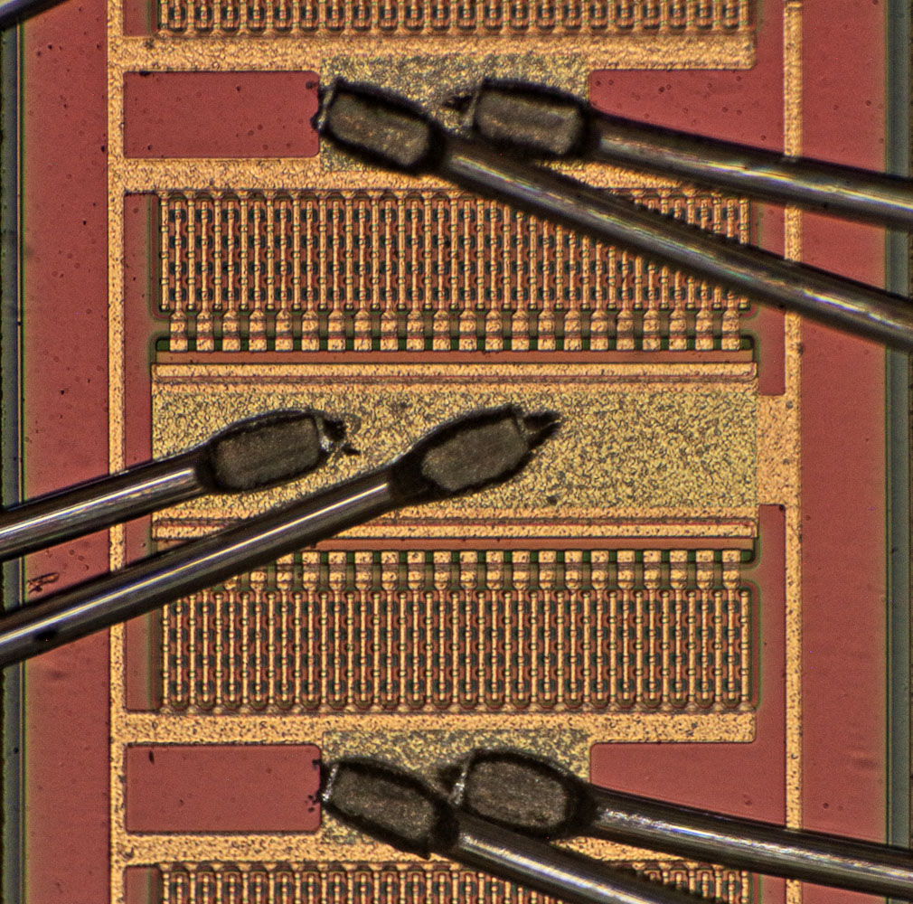
I don´t think they did some tuning here. In my view it looks more like some bond problems.
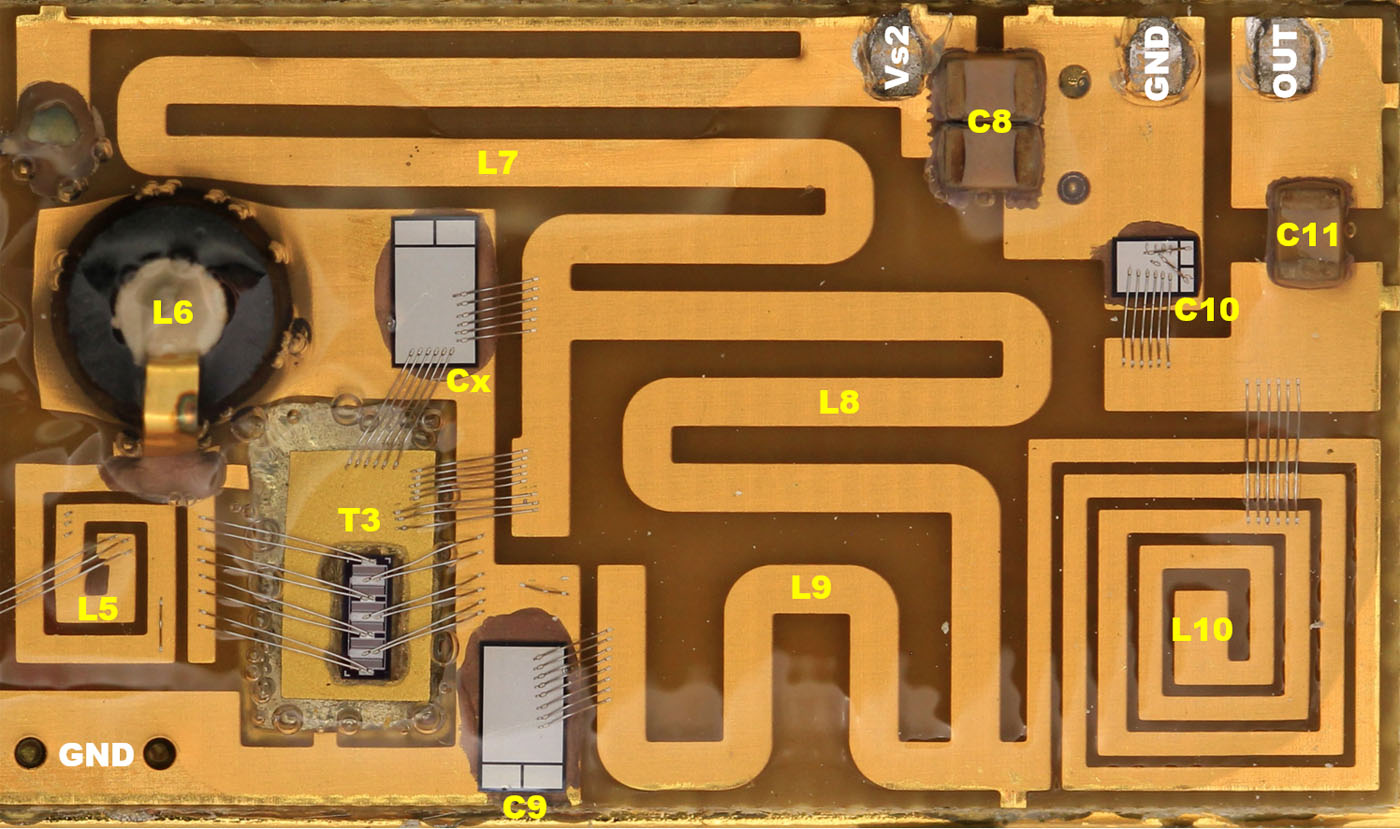
On the right side there is the output stage.
That looks like some tuning. The first bond connection was cut and a new bond connection was established at a different place.
L6 has a core because you need a lot of inductance at this place.
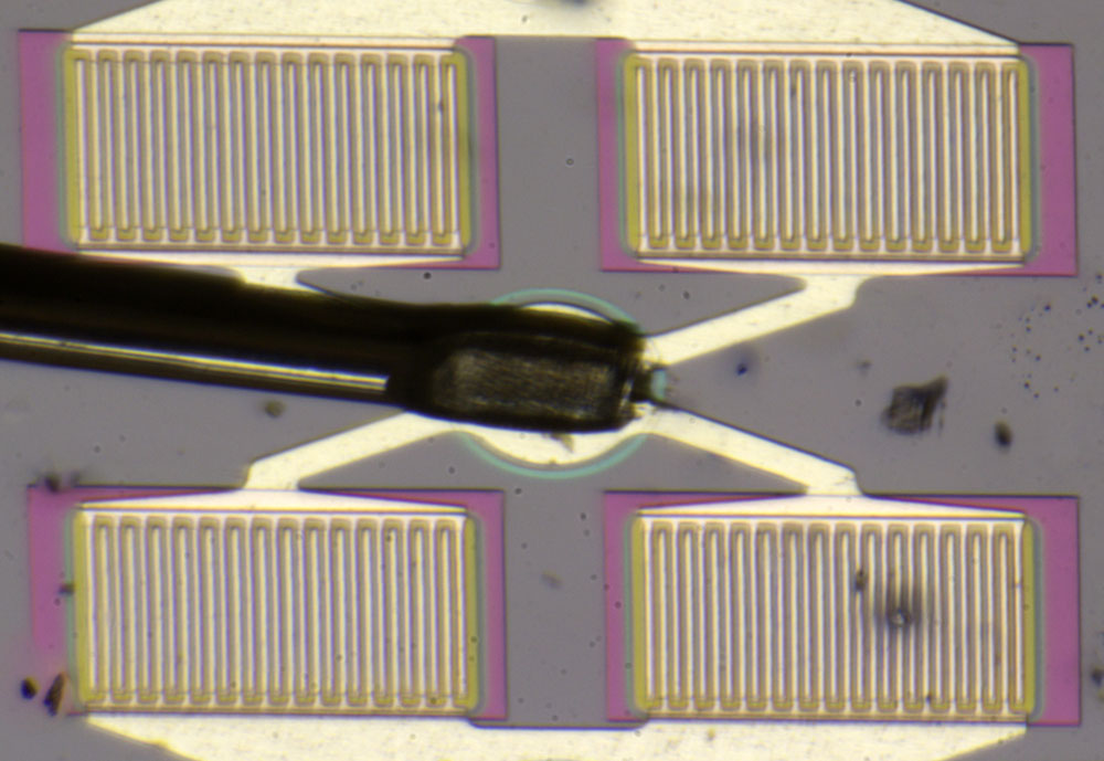
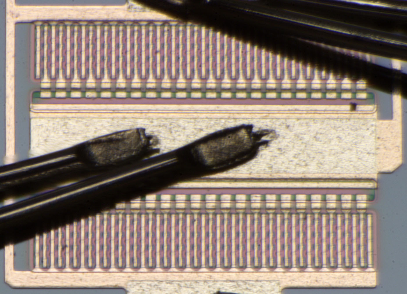
The output transistor T3 sits on a second BeO ceramic. The currents are below 1A but you need a lot of connections to get a low parasitic inductance.
T3 is an overlay transistor like we have seen it in the 2N3553 (
https://www.richis-lab.de/Bipolar22.htm).
Every vertical emitter line has an emitter resistor and the whole block is connected to one single horizontal emitter resistor. That´s important to get a uniform current distribution.
https://www.richis-lab.de/rfamp01.htm 


