Author Topic: ADCs - die pictures  (Read 3101 times)

0 Members and 1 Guest are viewing this topic.

Offline NoopyTopic starter

  • Super Contributor
  • ***
  • Posts: 1816
  • Country: de
    • Richis-Lab
ADCs - die pictures
« on: December 17, 2020, 12:17:42 pm »
After some DACs (https://www.eevblog.com/forum/projects/dacs-die-pictures/msg2999142/#msg2999142) we need a topic for ADCs!  8)

The overview on my website can be found here: https://richis-lab.de/ADC.htm


So let´s start with the ADC574:


Inside the ADC574 there are two dies...


...a digital die...


...and an analog die.


The analog die is 5,1mm x 2,6mm.


It was designed by Harris.


I assume the brownish resistors have lower resistances than the the green ones which are connected in serial. This makes it easier to tune the resistance near the ideal value.


The DAC contains seven current sinks (A-G) for the three MSBs.
The nine LSBs are switching the current sinks 0-8 which are connected to a R2R network for scaling the currents.
REF is the reference current sink.
X sinks a constant not switchable current. I assume that compensates leackage currents.


On top of the current sinks there is some control circuit generating a differential signal (red/green).
In the middle there are two resistor types for tuning followed by the current sink transistor. The transistor is controlled by the yellow potential.
In the lower part there are the two transistors which switch the current from the R2R-ladder to the dummy load.


Dummy-R2R and R2R


The input signal (yellow) is mixed with the DAC output (blue) giving the green potential that is connected to the comparator on the right side where it is compared with ground (red). The comparator contains testpads and tunable resistors which make it possible to tune the threshold. On the upper edge there ist the differential output.


The digital die is 4,0mm x 2,1mm and was also built by Harris.


A lot more pictures here:

https://richis-lab.de/ADC02.htm

 :-/O
 
The following users thanked this post: TiN, mikerj, exe, RoGeorge, wergor

Offline NoopyTopic starter

  • Super Contributor
  • ***
  • Posts: 1816
  • Country: de
    • Richis-Lab
Re: ADCs - die pictures
« Reply #1 on: October 31, 2021, 10:01:20 pm »
PART 1
You will need some time to read this.  ;D


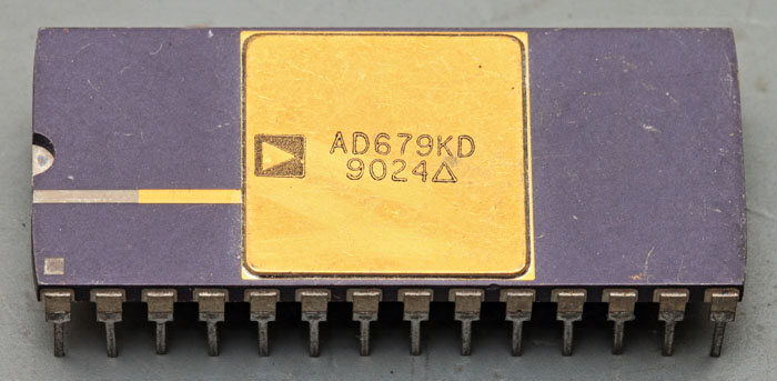
The Analog Devices AD679 is a 14Bit subranging SAR Analog Digital Converter.
There are six different versions: A, B, J, K, S, T. K gives you the best specifications. T can work in an temperature range between -55°C and 155°C.


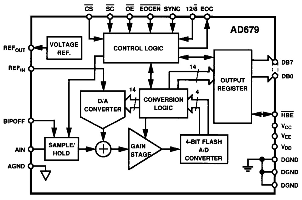
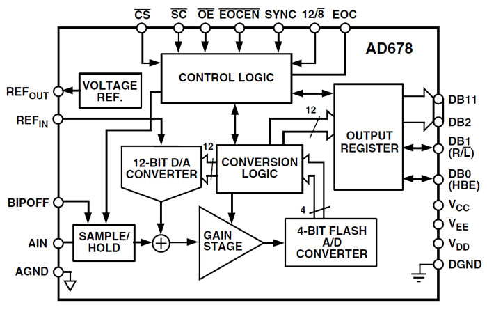
The datasheet shows the architecture of the AD679. In the first place there is a Sample&Hold stage giving you 10M/10pF input impedance. The input signal is fed into a summing node from which a DAC draws current. That´s a normal SAR ADC but instead of a comparator the AD679 uses a 4Bit-Flash-ADC with an amplifier that quantifies the residual signal. With this architecture the AD679 needs just five cycles to get 14Bit while a normal SAR-ADC would need 14 cycles.
(There is a 12/8 pin. In the AD679 pinning you won´t find a 12/8 pin. Furthermore there is no explanation for the 12/8 pin in the datasheet. We will see...)


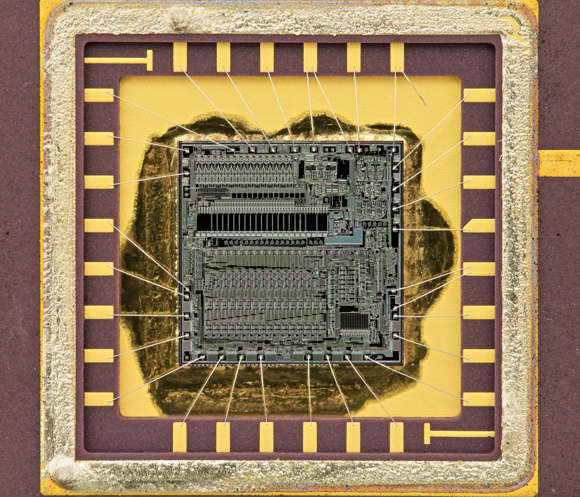
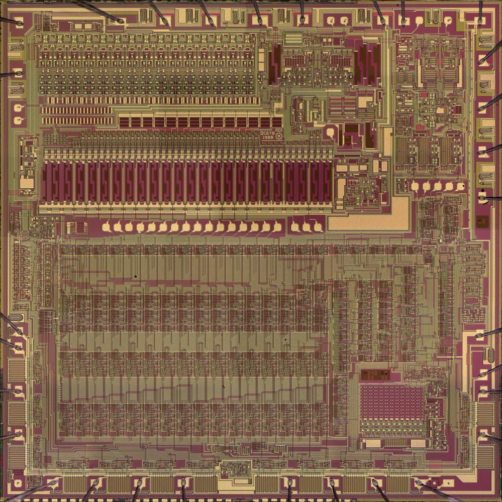
The die is really big (6,5mm edge length).


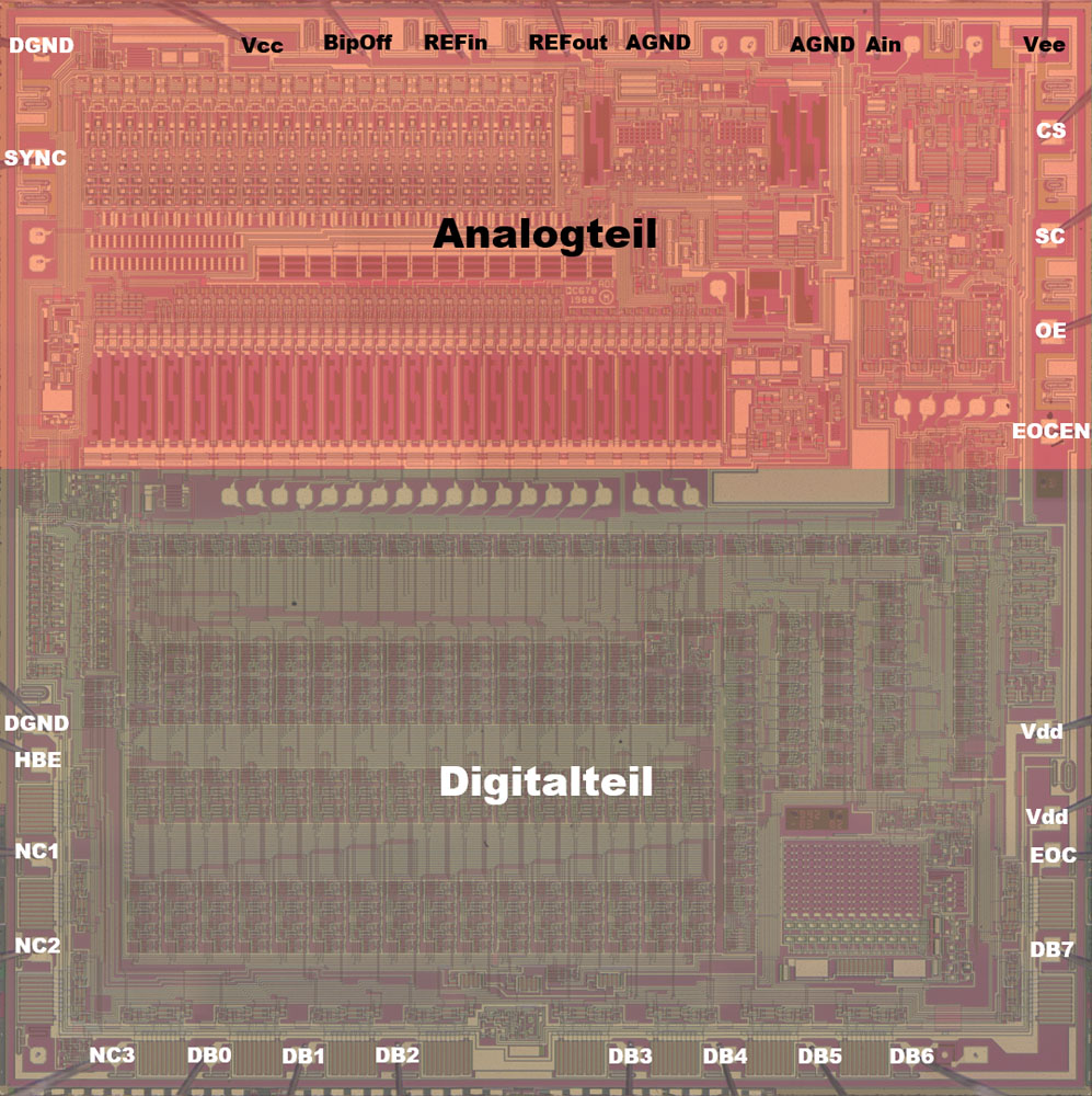
The digital part is a little bigger than the analog part.


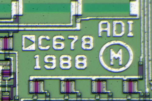
It looks like the AD679 was designed in 1988.
C678? AD678?


The AD678 is nearly the same as the AD679. While the AD679 converts 14Bit with a sample rate of 128kS/s the AD678 gives you 12Bit with a sample rate of 200kS/s.
(Now we know where the 12/8 pin comes from! Analog has copied it from the AD678 datasheet!)


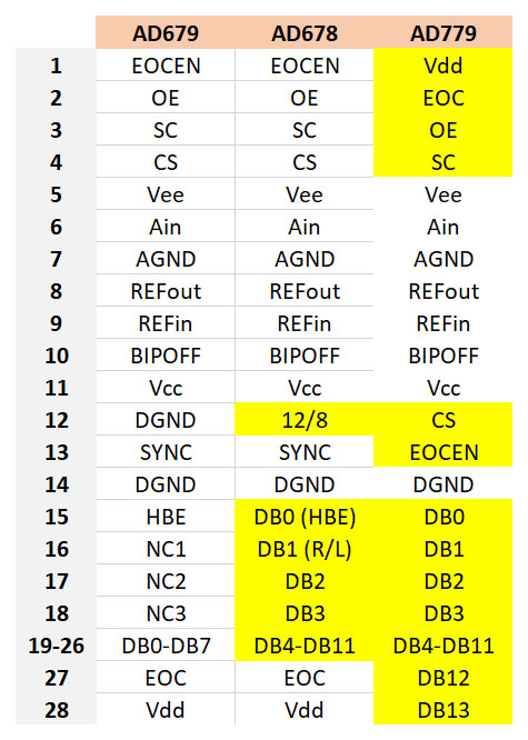
The pinning of the AD678 is quite similar to the AD679. The AD678 gives you the possibility to use a 12Bit interface and you can switch it to 8Bit (with the 12/8 pin). It looks like the AD678 and the AD679 use the same die.
There is also a AD779 with the same specifications as the AD679 but with a 14Bit interface. However the AD779 has to contain a different die because on the AD678 die there are just 13 outputs and you need one for EOC.


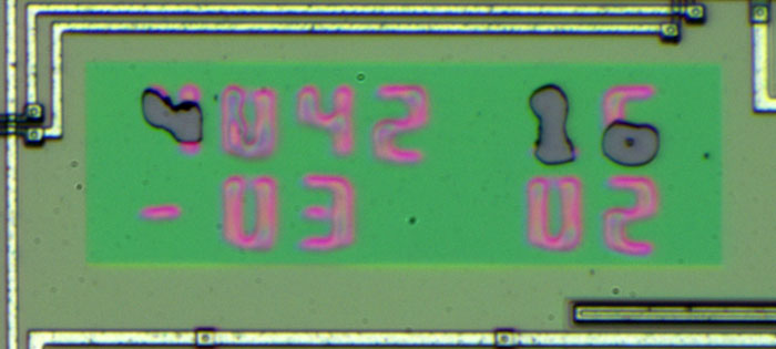
There are some laser tuned resistors on the die. You can find some numbers perhaps for binning perhaps to retrace the tuning process.
It seems like the passivation layer is damaged.


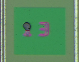
Like in most laser tuned circuits there is an additional bondpad with an tuneable rectangle to tune the tuning system.


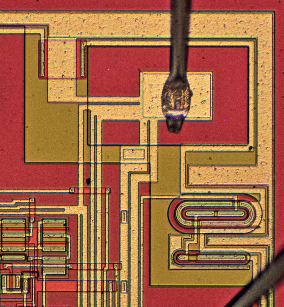
Some potentials (here Vee) are distributed with a lot of tracks that contain different star points.


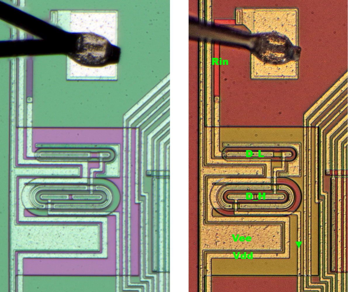
Here you can see the input protection, a series resistor followed by two diodes. Interesting detail: The metal line contacting the diodes is interrupted probably to force the current through the silicon and getting better overvoltage protection.


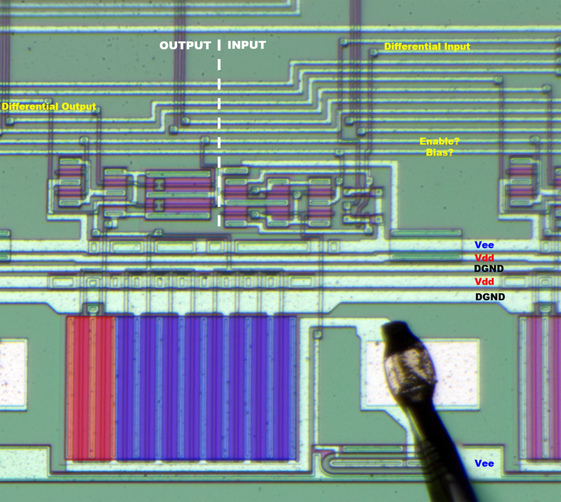
The output stages are easy to spot. They contain a small highside transistor (red) and a big lowside transistor. It seems there is an enable signal and a differential signal controlling the output.
Surprise: There is also an input stage with a differential output and a bias adjusting the threshold.
The output stages are supplied with exclusive Vdd and DGND lines.


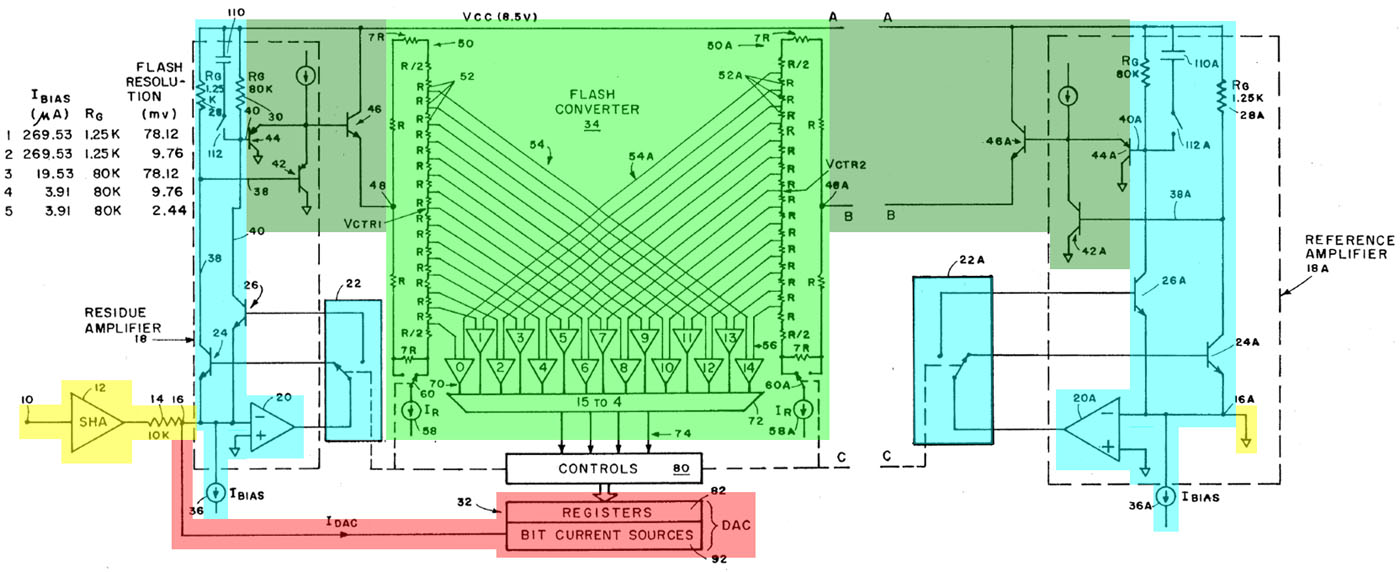
The datasheet refers to some patents. One of them is the US4804960 that contains an interesting schematic. Most of the circuit is symmetrical.
Yellow: On the left side there is the S&H circuit and a 10k resistor that converts the voltage into a current.
Red: The DAC sinks a current out of the summing node to compensate the input current as good as possible.
Cyan: The residual current is amplified with different amplification factors. The opamp 20 and the transistor 24 (or 26) do the amplification. The current sink 36 sets a bias current.
Dark green: Between the amplifier and the FADC there is a buffer stage.
Green: The FADC is built with 15 comparators and two resistor strings. The current sink 58 determines the resolution of the FDAC. The buffer transistor 46 lifts and sinks the complete resistor string. On the right side there is the same circuit supplying the comparators with the reference potential. This criss-cross arrangement compensates a lot of errors and drift effects. The LSBs are generated in the middle of the resistor strings.

The FADC has to measure smaller voltages each cycle.
In the second cycle the current sink 58 is switched by the switch 60. The current in the resistor string is divided by 8 and the resolution is eight times higher.
In the third cycle switch 60 is switched back and the amplifier is switched to transistor 26. The higher collector resistor gives us a amplification of 64.
In the fourth cycle the switch 60 is switched into the higher resolution again. Additionally switch 110 is closed to reduce the bandwidth from 6MHz to 800kHz. The conversion speed is reduced but also the noise is reduced.
In the fifth cycle the current through the resistor string is reduced further by a factor of 4.
The bias current 36 is adjusted too.


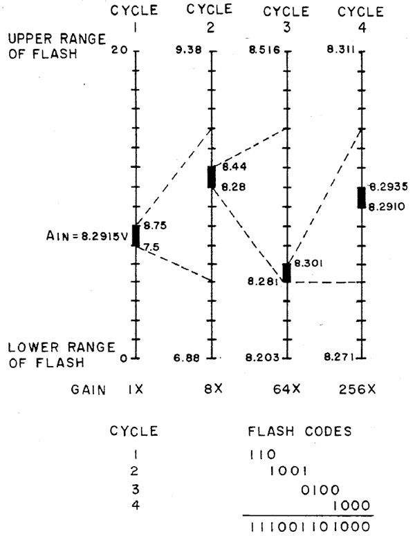
The patent shows one conversion. The FADC gives us a 4Bit value of the input voltage. The first three Bits of the DAC are configured with this value reducing the current in the summing node. In the next cycle the FADC gives us the next 4Bit and so on... In the last cycle (not shown here) the FADC adds the last 2Bit to the 12Bit value generated in the former cycles.
The Bits generated by the FADC are summed up to get the 12Bit value of the input signal. The FADC generates 4Bit but only 3Bit add up to the result. The fourth bit is for error correction. It can switch the LSB of the former 4Bit. That´s not a digital correction. Some of the current sinks in the DAC are doubled up.


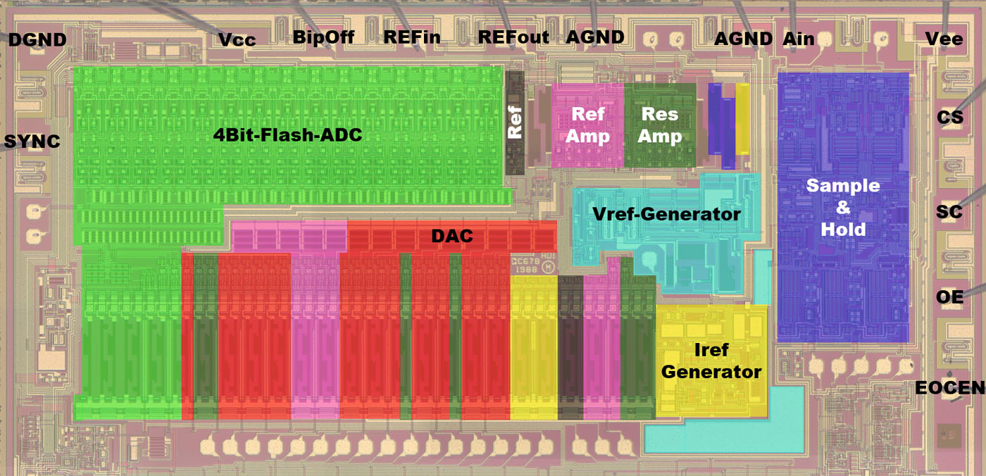
In the analog part of the die the Sample&Hold stage is on the right side (blue). A differential signal is fed to two resistors right of the residual voltage amplifier (dark green). Left of the amplifier is the reference amplifier (pink). Under the amplifiers there is the voltage reference (cyan) and the reference current generator (yellow). There is a active regulated reference potential on the die (black). The red area is the DAC. The FADC (green) consumes a lot of area although it converts just 4Bit.

Next part coming soon!

 
The following users thanked this post: doktor pyta, RoGeorge, MegaVolt

Offline NoopyTopic starter

  • Super Contributor
  • ***
  • Posts: 1816
  • Country: de
    • Richis-Lab
Re: ADCs - die pictures
« Reply #2 on: October 31, 2021, 10:02:30 pm »
PART 2


The S&H stage has to provide a high input impedance and a fast switching while the error budget of the whole 14Bit ADC is just +/-0,6mV.


In the datasheet of the AD679 the patent US4833345 is mentioned. It contains the S&H stage. I have put some color in the schematic to explain the signal processing.
In the sample state the input voltage travels over the red lines. The feedback signal travels over the blue lines. The trick is that in the hold state the signal and the reference path are switched. Due to the switching a lot of the offset errors are compensated.
Another compensation device is the transistor 38 with the capacitor 42. Going to hold state transistor 30 is switched off and some of the charges of the sampling capacitor 18 are transferred into this switch. To compensate this loss of charges transistor 38 and capacitor 42 are integrated. While switching off the transistor the same amount of charges flow into 38 and the capacitor generates the lost voltage.
The bulk potentials of the transistors 30 and 38 are on a fixed potential above the input signal. The gate potentials are floating on top of the input signal too. => roughly ideal switching


You can spot the S&H stage quite easily. The analog input is fed to the circuit from above. At the lower edge the digital area supplies the circuit with some control signals with five testpads. In the upper left corner you can find the differential output.


Analog Devices made quite some effort to distribute important voltages. Here you can see Vee. On the right edge one line connects the substrate with a lot of vias probably to guard the circuit against the bondpads. One line is connected with the voltage reference but it is also connected to the substrate at the lower area of the S&H circuit (yellow). Another line is used for local substrate contacts (blue) and isolation trenches and some circuits (blue/red). There are two more Vee lines supplying the circuit (marked orange just at the star point).


Drivers for 20, 30, 38.


The input stage is somehow differential.


You can´t identify every part of the circuit but here you can see the sampling capacitor 18 and the compensation capacitor 42.


Here we can find the double switch 20. It´s built with the two double transistors above and below the capacitor in the middle of the picture.
Around the switches they integrated the two opamps 22 and 26.
The two capacitors in the left corners are the capacitors Cc and Cc´. There is just one electrode, the other one is the substrate.


Next part coming soon!

 
The following users thanked this post: RoGeorge

Offline NoopyTopic starter

  • Super Contributor
  • ***
  • Posts: 1816
  • Country: de
    • Richis-Lab
Re: ADCs - die pictures
« Reply #3 on: October 31, 2021, 10:03:36 pm »
PART 3


On the right side you can see the amplifier for the residual signal in the summing node. On the left side there is the reference amplifier.
Left and right of the amplifiers there are two tuneable resistors. On the right side there is the summing node that sums up the output of the S&H stage, the bipolar offset, the DAC current (and the bias current 36).
The bigger circuit above the amplifiers seems to be a voltage regulator.
The collector resistors 28 and 30 are built with a lot of small resistors. Left of the resistors you can see the capacitor for the bandwidth limiting. There is not only a transistor connecting it to the resistor 30 but also a transistor connecting it to the output.
The transistors are isolated with a grid of isolation trenches. Two of the current sinks in the DAC area are used for switching the amplification factor (22/22A), two are used as constant bias, two more are used as switched bias (36).


This circuit generates a regulated reference out of Vcc and AGND so the different states don´t mess AGND. There is a star point with feedback (blue).
The active reference is used for the R2R divider of the DAC and as a dummy load for the inactive current sinks. In addition it is connected to the second line of the differential output of the S&H stage.

There are three overvoltage protection circuits (green) connected to AGND. Two circuits protect the inputs of the two amplifiers. The third one protects the second output of the S&H stage.


Next part coming soon!

 
The following users thanked this post: RoGeorge

Offline NoopyTopic starter

  • Super Contributor
  • ***
  • Posts: 1816
  • Country: de
    • Richis-Lab
Re: ADCs - die pictures
« Reply #4 on: October 31, 2021, 10:04:40 pm »
PART 4


The DAC uses most of the prominent current sinks. There is a R2R current divider. Just the three current sinks A, B and C sink their current directly. You can see the groups of current sinks with the doubled current sinks for error correction (red). With the information in the patent US4804960 we know one current sink sinks 125µA. To achieve 14Bit the error of the currents must stay below +/-31nA.


Some of the current sinks are connected to the two amplifiers of the FADC. For the reference amplifier Analog integrated even a second R2R current divider.
4, 6 and B are the bias current sinks named 36 in the patent. Ib is a constant current bias. 22 and 22A switch the amplification factor.


Here we have one current sink. In the middle is a tuneable resistor. There are bigger and smaller areas to do coarse and fine tuning.
On the lower end the current sink connects to Vee. There is an additional MOSFET probably to do some regulation.
The resistor area is connected to Vcc to get a good isolation.


Above the current regulating transistor (yellow) there is a MOSFET working as cascode (green) to isolate the current sink towards voltage fluctuations. The blue circuit is the control circuit for the toggle switch (cyan).


Four current sinks generate the reference current. There are additional thin areas around the resistors that look like shielding but they are connected to Vee and the current sink input. It seems like the additional area is a startup resistor with a high resistance.


Here we see the bandgap reference of the AD679. There is the characteristic transistor pair with a bigger transistor around a smaller transistor (red). The white transistors mirror the current through the two transistors. With the yellow resistors you can tune the temperature coefficient. The orange resistor is connected to a testpad and you can measure the current trough the bandgap transistors. Three transistors (cyan) are the output of the reference that is connected to the REFout (blue). There is a sense line (green) that is connected to a resistor divider (pink) that adjusts the output voltage. There is quite a big capacitor (black).


The smaller capacitor at the bandgap reference is connected to a bigger one under the circuit that controls the current flow through the current sinks.


The control line for the current sinks is connected to the middle of the current sink area to reduce the voltage drop to the last one.


Next part coming soon!

 
The following users thanked this post: RoGeorge

Offline NoopyTopic starter

  • Super Contributor
  • ***
  • Posts: 1816
  • Country: de
    • Richis-Lab
Re: ADCs - die pictures
« Reply #5 on: October 31, 2021, 10:05:47 pm »
PART 5


The FADC consumes quite some area of the die. On the left side there are two testpads to measure the input of the FADC.


There are two resistor strings connected to the amplifiers and the FADC. Each resistor string gives you the resistances 1/2R, 7R, R, R, 7R, 1/2R.
The current sinks 58 and 58A are a little more complex than the schematic in the patent circuit.


There are two current sinks for each FADC resistor string.
The current sinks are switched in a manner that the buffer always has to deliver the same current while the current through the resistor string is reduced to raise the resolution.


The resistor strings of the FADC are interweaved under the comparators.


Each comparator is connected with its neighbour. At the point where the status of the comparators change a small circuit is activated that outputs the correct digital value on the 4Bit data line.


The small circuits on the FADC data lines contain four emitters. Only some emitters are connected to the data line so you get the digital output you want.


Next part coming soon!

 
The following users thanked this post: RoGeorge

Offline NoopyTopic starter

  • Super Contributor
  • ***
  • Posts: 1816
  • Country: de
    • Richis-Lab
Re: ADCs - die pictures
« Reply #6 on: October 31, 2021, 10:06:52 pm »
PART 6


The digital part of the AD679 is quite big. The structures are big enough to analyze the complete program but it would take quite some time and we won´t get a lot of additional information.


Analog Devices didn´t use the normal gatearray structures. There are modules which are quite similar. Here we see one of them with a lot of NAND-Gates. You can´t use every NAND-Gate independently because the gates of the 4* 6-IN NANDs are connected and there is just one pull-up structure for each of these NANDs.


That is interesting: Where the FADC output reaches the logic area you can switch to the bondpads NC3, DB0, DB1 und DB2. Perhaps that was used for tuning the circuit.


In the lower area there are twelve similar circuits (red) that are connected to HBE, NC1-NC3 and DB0-DB7. Left of the red area there are four more circuits. This row has to work like a shift register to get the data out of the AD679.
I´m sure you just have to burn some links to change a AD679 into a AD678. That´s reasonable because you can check the quality of the die and if it is not good enough for a AD679 you make it a AD678.


It seems like that circuit is the internal oscillator. There is a big tuned resistor grid. Analog Devices probably tuned the working clock.


A few more pictures and words:

https://www.richis-lab.de/ADC03.htm

 :-/O
 
The following users thanked this post: RoGeorge

Offline RoGeorge

  • Super Contributor
  • ***
  • Posts: 6437
  • Country: ro
Re: ADCs - die pictures
« Reply #7 on: October 31, 2021, 10:09:20 pm »
Wow, ADCs, subscribed, and thanks for all the pics!   :D
 
The following users thanked this post: Noopy

Online magic

  • Super Contributor
  • ***
  • Posts: 6897
  • Country: pl
Re: ADCs - die pictures
« Reply #8 on: November 01, 2021, 07:37:15 am »
Crazy :scared: :-+

So that's some sort of noncomplementary-Bi-complementary-MOS process, did I get it right?
There are the ordinary NPNs and lateral PNPs all over the place.
The lighter colored MOS are N-ch and the darker ones are P-ch, it seems.
Don't think I have seen a single JFET anywhere.
 

Offline NoopyTopic starter

  • Super Contributor
  • ***
  • Posts: 1816
  • Country: de
    • Richis-Lab
Re: ADCs - die pictures
« Reply #9 on: November 01, 2021, 08:08:34 am »
Crazy :scared: :-+

So that's some sort of noncomplementary-Bi-complementary-MOS process, did I get it right?
There are the ordinary NPNs and lateral PNPs all over the place.
The lighter colored MOS are N-ch and the darker ones are P-ch, it seems.
Don't think I have seen a single JFET anywhere.

You are right on all counts.  :-+ :)

Online David Hess

  • Super Contributor
  • ***
  • Posts: 16858
  • Country: us
  • DavidH
Re: ADCs - die pictures
« Reply #10 on: November 01, 2021, 11:45:57 pm »
So that's some sort of noncomplementary-Bi-complementary-MOS process, did I get it right?
There are the ordinary NPNs and lateral PNPs all over the place.
The lighter colored MOS are N-ch and the darker ones are P-ch, it seems.
Don't think I have seen a single JFET anywhere.

Wouldn't JFETs require separate steps for ion-implantation?  They would avoid that if at all possible.

Are there any CMOS processes which also included JFETs?
 

Online T3sl4co1l

  • Super Contributor
  • ***
  • Posts: 21913
  • Country: us
  • Expert, Analog Electronics, PCB Layout, EMC
    • Seven Transistor Labs
Re: ADCs - die pictures
« Reply #11 on: November 02, 2021, 12:46:18 am »
Other than a substrate JFET, I think was pretty easy/common?  (Mainly just used for starting bias into a bandgap or whatever.)

Tim
Seven Transistor Labs, LLC
Electronic design, from concept to prototype.
Bringing a project to life?  Send me a message!
 

Offline NoopyTopic starter

  • Super Contributor
  • ***
  • Posts: 1816
  • Country: de
    • Richis-Lab
Re: ADCs - die pictures
« Reply #12 on: November 03, 2021, 08:49:04 am »
I agree with Tim. The easy way J-FET is easy to integrate but it's just good enough for start-up...

Offline NoopyTopic starter

  • Super Contributor
  • ***
  • Posts: 1816
  • Country: de
    • Richis-Lab
Re: ADCs - die pictures
« Reply #13 on: June 14, 2022, 07:36:32 pm »


The MAX111 is a delta-sigma ADC built by Maxim. It requires no additional components and can be connected directly to a microcontroller. The MAX111 delivers a digital value with a resolution of 12Bit every 20ms at maximum or a resolution of 14Bit every 200ms. In addition, there is a sign bit and an overflow bit that indicates that the input level exceeds the normal range. The datasheet specifies the MAX111 as a +/-14bit ADC with a 12bit accuracy. Strictly speaking the signed output provides 15Bit. Nevertheless the designation +/-14Bit is more appropriate, since reading in negative values is just possible due to the differential input and the resolution is actually only 14Bit.

The MAX111 gets by with a single 5V supply and can convert differentially +/-1.5V. However no negative voltages in relation to the GND are allowed. The -1.5V refers to the voltage between the differential inputs. In addition to the MAX111, the data sheet also lists the MAX110, which converts +/-3V with a +/-5V supply. Current draw is around 1mA, dropping to a maximum of 10µA in power down mode.

The AC bin has the lowest errors. The datasheet specifies a non-linearity of +/-0.03% of full scale (for an input voltage less than 0.667 * Uref). The offset error may be up to +/-4mV. The full-scale error can be limited to +/-0.2% by the integrated calibration rutine. Without adjustment you have to deal with -8%/+0%.


The datasheet contains a block diagram. The ADC provides two differential inputs. A multiplexer allows switching between the two inputs and the reference voltage. The maximum bias current is 0.5mA. The input capacitance is 10pF.

As usual for a delta-sigma ADC, the opamp at the input feeds an integrator. A comparator evaluates the output of the integrator and controls the polarity of the reference voltage at the input of a second operational amplifier. Its output is connected to the integrator too.

The comparator outputs one logic level until the lower operational amplifier causes the comparator to switch through the integrator. The output of the lower operational amplifier changes polarity accordingly and the integrator is recharged until the comparator switches again. During this process, the input signal sets the switching time. At the output of the comparator there is a square wave modulated according to the input signal. That´s already a digital data stream.

The converted data is averaged over up to 102,400 clock cycles resulting in a relatively noise-free digital value. The dither generator ensures a slight variation of the switching times. Otherwise the switching operations would generate noise that can´t be filtered.

The MAX111 contains all the necessary additional circuit parts to allow it to be easily connected directly to a controller. Among them is a clock generator that can be used as an alternative to an external clock.


The datasheet contains an image of the die. It also states that 5849 transistors were integrated in the MAX111.


The die included in the package corresponds to the illustration in the datasheet. The dimensions are approximately 4.2mm x 3.0mm.


The design dates back to 1994.

AD67W could be the internal designation of the design. 1Z could be a variation of the metal layer that allows switching between the MAXIM110 and MAX111.


The revisions of eight masks can be found on the die.


Some elements of the block diagram can be identified on the die.


The multiplexer which switches between the two inputs and the reference potentials is located directly next to the bondpads on the left side. Two lines run vertically which finally lead to one of the opamps. From reference inputs two additional lines lead to the second opamp.


The details of the two opamps cannot be analyzed, but the large symmetrical structures are clearly visible.

To the right of the operational amplifiers there must be the comparator. However an assignment to certain circuit parts is not possible.


A large area is occupied by a capacitor consisting of four individual elements. Most likely, this is the capacitance of the integrator.


The dither generator appears to be located in the upper left corner of the die. It is a isolated small circuit whose output leads to the area where the comparator is probably located. Often the noise of a Z-diode serves as a basis for such a dither generator.


The logic area looks like a gatearray. The two supply potentials are fed in from above and below. Between the vertically lined up logic elements are the connection lines that realize the logic links. However, the structures are not quite as regular as in a gatearray. This made it possible to use the area more efficiently.


The internal RC oscillator is located in the lower right corner. The bondpad of the XCLK pin is also placed there. It outputs the internal clock or accepts an external clock. With the help of three testpads you can trigger two metal fuses during production. Most likely the frequency of the RC oscillator can be adjusted with this fuses.


https://www.richis-lab.de/ADC04.htm

 :-/O
 
The following users thanked this post: RoGeorge

Offline NoopyTopic starter

  • Super Contributor
  • ***
  • Posts: 1816
  • Country: de
    • Richis-Lab
Re: ADCs - die pictures
« Reply #14 on: July 19, 2022, 07:56:20 pm »


Now that is an ADC!  ;D

The ADC-12QZ is a SAR ADC with a resolution of 12Bit. In 1972 Analog Devices sold this device for 92$ with a purchase of 100 pieces. For smaller quantities a price of $129 can be found. The optional input buffer amplifier is not yet included. With the input buffer, the price increased by 20$ for small quantities. All in all this results in a price of 1056$ (2022) converted to today's purchasing power. Several manufacturers later had pincompatible alternatives in their product line.

The ADC-12QZ converts an analog value every 40µs and offers a linearity of +/-0,5LSB. The temperature drift of the offset is +/-10ppm/°C. The gain factor drifts with +/-30ppm/°C. The device requires -15V, +5V and +15V. The possible input voltage range is from -10V to +10V. The input resistance with input buffer is 1GΩ, without input buffer it is just 2,5kΩ to 10kΩ depending on the input voltage range. The converted digital value is output in parallel and serial.

A datecode is printed on the lower side of the case and refers to calendar week 39 of 1984.

In addition to the 12Bit ADC Analog Devices sold the ADC-8S and ADC-10Z with resolutions of 8Bit and 10Bit. Apart from the resolution the specifications are very similar with the ADC-8S converting remarkably slowly. According to the datasheet one conversion can take up to 1ms. However, this time is just needed at full scale. At lower input levels the conversion is faster. A diagram printed in the datasheet shows that the ADC-8S does not behave like a classic SAR ADC. Instead the DAC ascends a staircase with a constant step height of one LSB. Consequently, with a resolution of 8Bit up to 256 steps have to be passed until the value of the input signal is reached. The unit price for the ADC-8S was 79$ (2022: 560$). The input buffer is always integrated in this device. The unit price for the ADC-10Z including the input buffer was $119 (2022: $844).


The case measures 10,2cm x 5,1cm x 1,0cm. There would be room for a total of 72 pins on the long edges. The ADC-12QZ has 35 pins. The lid has holes for more but not for all 72 possible pins. Over a rectangular cutout the device has been potted with a white silicone-like compound.


The ADC-12QZ contains all circuit parts necessary for an analog-to-digital conversion. In the upper part of the schematic the datasheet shows the optional input amplifier. The input signal is ultimately routed to the DAC via pin 5 or pin 6. Pin 1 allows to adjust the gain of the DAC and thus the ADC. As will be shown the "High Gain Ref Amp" is located inside the DAC. The input voltage range of the ADC-12QZ can be adjusted by a different connecting of pins 5, 6 and 19. Behind pins 5 and 6 are resistors of different sizes, which convert the input voltage into currents of different sizes. Pin 19 can be used to set an additional current and thus an offset.

The node where the currents of the input signal, the DAC and the offset input come together is connected to the comparator of the ADC and to pin 20. This is also the location of the analog signal ground, which ensures that the comparator can operate with as little interference as possible. A reference voltage source is integrated in the ADC-12QZ, too, whose potential is applied to pin 22.

The digital part of the ADC is shown in the lower area. A TTL logic checks the output of the comparator and controls the DAC according to the SAR principle. Depending on the output of the comparator the inputs of the DAC are activated or remain inactive starting at the MSB. This causes the output of the DAC and thus the digital value to approach the input signal. After 12 cycles the final value is reached. The control signals of the DAC are simultaneously routed directly to the output pins. The MSB is additionally available inverted. This is useful in bipolar operation, where you can alternatively tap the output value as a complementary number.

The ADC-12QZ has an internal clock generator. Via pin 35 it is possible to alternatively feed in an external clock signal. In addition to parallel data output, the device provides a serial output too. A digital ground potential keeps the interference of the logic away from the analog circuit parts.


The ADC-12QZ consists of a thin PCB that carries the connector pins and is potted upside down in the two-piece package.


The silicone encapsulation can be removed relatively well. Only on the bottom of the PCB the silicone sticks more strongly.

Since the ADC-12QZ was already produced for 12 years in 1984 it may well be that earlier models were built differently.


The pins of the components were shortened so that they do not stand out too far from the board. On the metal housings the tabs that serve to assign the pins have been bent over.


The core of the ADC-12QZ is the 12bit DAC AD562 (https://www.richis-lab.de/DAC19.htm). The reference voltage generation is based on the temperature compensated zener diode 1N829A (https://www.richis-lab.de/REF22.htm). The voltage of the zener diode is scaled appropriately via the operational amplifier AD741 (https://www.richis-lab.de/Opamp50.htm). The reference voltage is stabilized with a film capacitor and a ceramic capacitor and serves at the same time as supply for the zener diode. The non-scaled reference voltage of the zener diode is applied to pin 22. Most likely the interface serves to stabilize the potential with a capacitance.

In the lower right corner the input buffer is placed. It is an LM310 (https://www.richis-lab.de/Opamp52.htm). In the supply line there is a film capacitor, which is actually needed mainly for the input buffer. The ADC is designed in such a way that the current consumption remains relatively constant. The current consumption of the input buffer, on the other hand, changes with the input level. The comparator, an LM211 (https://www.richis-lab.de/Opamp51.htm), is located in the center of the board as an interface between the analog and digital sections.

In the digital part there is a SN7400 (https://www.richis-lab.de/logic14.htm), a SN7402 (https://www.richis-lab.de/logic15.htm), a SN7404 (https://www.richis-lab.de/logic16.htm), a SN7474 (https://www.richis-lab.de/logic17.htm), a SN7493 (https://www.richis-lab.de/logic18.htm) and two 9334s (https://www.richis-lab.de/logic19.htm). The 9334s store the current value during digital conversion, supply it to the DAC and output it via the parallel interface. A single 2N2222 (https://www.richis-lab.de/BipolarA08.htm) generates the inverted MSB. In the supply of the digital part, there is another film capacitor on the right edge. The placement doesn't seem very logical, since the current could cause interference on its way through the analog part. However, since several small ceramic capacitors are placed in the digital part, the problematic high-frequency interferences are already strongly attenuated there.


https://www.richis-lab.de/ADC05.htm

 :-/O
 
The following users thanked this post: TiN, doktor pyta, RoGeorge

Online David Hess

  • Super Contributor
  • ***
  • Posts: 16858
  • Country: us
  • DavidH
Re: ADCs - die pictures
« Reply #15 on: July 19, 2022, 08:30:06 pm »
Analog Devices had a little bit to say about the ADC-12QZ in their book.
 

Offline NoopyTopic starter

  • Super Contributor
  • ***
  • Posts: 1816
  • Country: de
    • Richis-Lab
Re: ADCs - die pictures
« Reply #16 on: December 04, 2022, 08:04:33 pm »


The LTC2412 is a Delta-Sigma-ADC that provides 24Bit resolution on two differential inputs. The accuracy is of course much lower. The datasheet specifies a non-linearity of 2ppm, a full scale deviation of 2,5ppm, an offset of 0,1ppm and a noise level of 0,16ppm. Whereby these are just the typical not the maximum values. The internal oscillator operates at 19,2kHz. Externally, a clock of up to 500kHz can be fed into the system. The conversion time is then 41ms. With a supply voltage of 2,7V to 5,5V the LTC2412 draws just 200µA during normal operation.


The blockdiagram in the datasheet shows the functions that are integrated in the LTC2412. The two differential inputs are switched to the input of the Delta-Sigma-ADC via a multiplexer. The reference voltage is supplied differentially too. The ADC is a third order Delta Sigma Modulator. This means that three modulators are connected in series, which improves the SNR. A digital filter follows before the data is finally output serially. The internal clock can be configured to filter out 50Hz or 60Hz interference as best as possible.


Yes that´s not the best picture I have taken up to know.  ::) The die of the LTC2412 is 3,1mm x 2,0mm. The design apparently dates back to 2001.

On the left is a large area with typical logic structures integrated. There the control and the digital filter is implemented. The digital interfaces are located at the lower edge of the die and are framed by two ground bondpads on both sides.

At the upper edge the three differential inputs are placed. In the right area, you can see three larger symmetrical structures, which are mainly noticeable because of their large capacitances. These are probably the three delta sigma modulators.

In the upper left corner there are 10 testpads connected to some resistors. It remains unclear what exactly they calibrated here.


https://www.richis-lab.de/ADC06.htm

 :-/O
« Last Edit: December 04, 2022, 09:23:38 pm by Noopy »
 
The following users thanked this post: RoGeorge


Share me

Digg  Facebook  SlashDot  Delicious  Technorati  Twitter  Google  Yahoo
Smf