However I doubt that one would see light from the buried junction. This would be rather deep inside the silicon so only very little of that light can escape.
I´m not sure about this.
A view days ago I tried to use a big KD501 transistor as a photovoltaic cell.
(https://richis-lab.de/Bipolar02.htm)
Across the base-emitter-junction I got the same current as across the base-collector-junction. It seems there wasn´t significant light reduction.
The normal avalanche process should also not produce light as the energy from the hot electron is used to generate new pairs. The normal recombination in silicon is without any light and if any it would be in the IR range (~ 1 µm). It would be only if a hot electron recombines or excites some defect in some way.
I agree with you that hot electrons generate new pairs but some of them will recombinate. Otherwise you will get a real breakdown with 0V and destruction of the junction. (I´m not absolutely sure about the last sentence but that would be my interpretation.)
The hot electrons can have a higher energy than you will see while normal current flow in the semiconductor. With "normal" current flow and "normal" recombination you don´t see any light. I agree with that. But in my view there is recombination of hot electrons.
I tried to take a "maximum tilted" picture but you can´t really say where the light is generated:
Several things to note here:
1) If the emission is happening underneath an oxide layer, let us remember that we call the silicon dioxide we encounter on an everyday basis "glass". No problems with light getting through centimetres of glass, let alone microns or 100s of nanometers.
2) The assumption made so far is that silicon is the emission candidate. What if it's the dopant? Several common dopants are very strongly associated with visible emission bands (common: arsenic, phosphorous, less common: gallium). There is, admittedly, very little dopant but we're seeing very little light.
3) The assumption that the material is "too thick" for emissions to make their way out. Remember that we are in the 100s - 1000s of nanometres territory here. At that scale one's assumptions brought from the normal scale world about opacity are quite likely to be wrong.
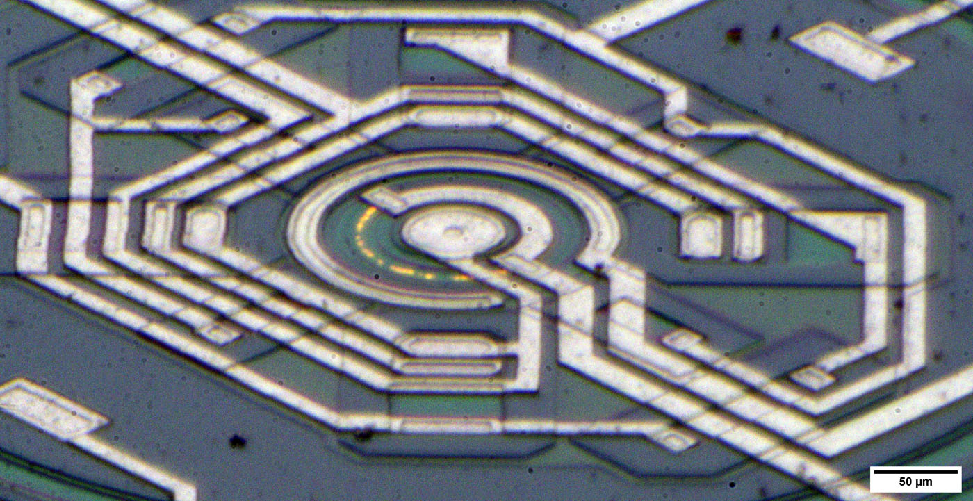
This diagram of the structure of the buried Zener from the LM399 might be instructive at this stage. It looks to me like the emission is happening well away from the region where the 'buried' junction action is supposed to be going on, perhaps between the outer ring of P- diffusion and the N- substrate or between the cathode and the surface part of the anode P- diffusion.


