Author Topic: A DIY semiconductor experiment  (Read 795 times)

0 Members and 1 Guest are viewing this topic.

Offline nebogeoTopic starter

  • Newbie
  • Posts: 7
  • Country: gb
    • Then Try This
A DIY semiconductor experiment
« on: September 07, 2024, 11:54:02 am »
Hi all, first time here - not sure where the right place to post this is, but I've been playing with simple DIY semiconductors a little.

I happen to live in a place (Cornwall) with a lot of naturally occurring minerals - more specifically a lot of non-ferrous metallic ores, which happen to have semiconductor properties. Historically material like galena (lead ore) was used to create the diodes in crystal radios.

I've been messing around a lot with pyrites and galena, but recently tried chalcocite (a secondary copper mineral) and noticed something interesting. Below is a curve trace in the way I think you 'normally' do it, using a sawtooth rising from -2.5V and 2.5V and plotting it against the current that passes through the crystal and a point contact 'cat's whisker':


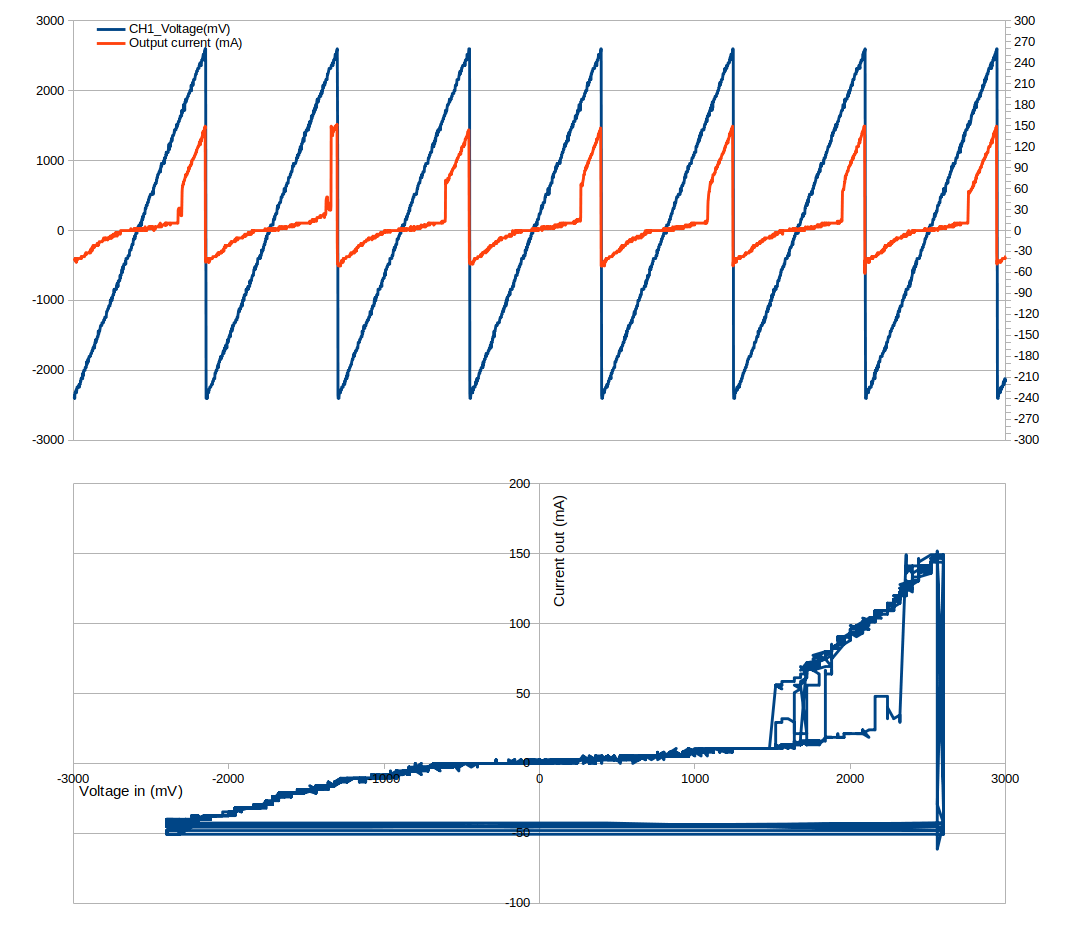
It's a bit rough and ready but we see (I think) is a rectifying behaviour where reverse voltage is (more or less) blocked and forward voltage starts conducting at a point between 1.5 and 2.5V.

I guess these relatively giant instabilities are to be expected in a few hundred million year old, naturally grown crystal that's been sitting in the rain on a mine dump for a few hundred years!

At some point I made a mistake and passed a sinewave through the crystal instead of a sawtooth, and I've noticed that the crystal does not "turn off" symmetrically, when the crystal is "turned on" and the voltage is dropping, it doesn't exhibit this threshold:


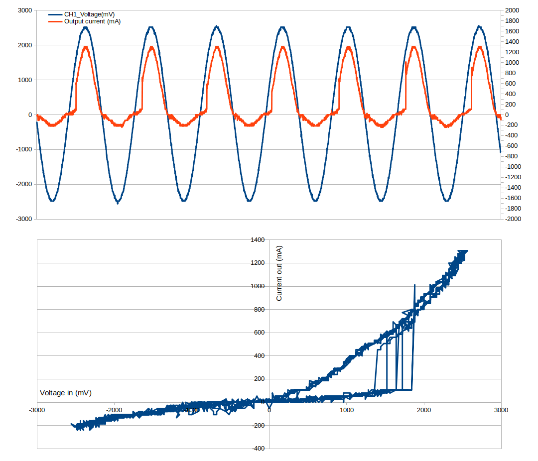
I presume this is a well known effect, I just can't find much about it online - or what it would be called.
 
The following users thanked this post: edavid, .RC., charles.ouweland, Slh, quince

Offline BrokenYugo

  • Super Contributor
  • ***
  • Posts: 1201
  • Country: us
Re: A DIY semiconductor experiment
« Reply #1 on: September 07, 2024, 01:58:07 pm »
Note you're working this diode about 1000x harder than a crystal set would. I would think a realistic IV plot for such a thing would end at 5-10mA forward current. The behavior right in the corner near zero is what actually makes a good "crystal detector" work
 
The following users thanked this post: nebogeo

Offline nebogeoTopic starter

  • Newbie
  • Posts: 7
  • Country: gb
    • Then Try This
Re: A DIY semiconductor experiment
« Reply #2 on: September 07, 2024, 02:27:12 pm »
This is a very good point, thank you - I'll try this! Similarly, I actually had a thought after posting that I could have the whole thing upside down, and the threshold shown could in fact be the reverse breakdown voltage.
 

Offline nebogeoTopic starter

  • Newbie
  • Posts: 7
  • Country: gb
    • Then Try This
Re: A DIY semiconductor experiment
« Reply #3 on: September 24, 2024, 06:08:06 pm »
A little update on this project (let me know if there is a more suitable forum for this sort of thing).

I tried reducing the current by a couple of orders of magnitude, but it essentially stops semiconducting as far as I could tell - I need to pump quite a bit through this material to see any effect. I may well be making a simple mistake here, but I will also try galena, which was more commonly used for crystal radio purposes and may just be far more sensitive.

In the meantime here is a plot of pyrite, a far more common mineral ('fools gold') and a fairly typical curve showing only a mild effect:


And this one is chalcopyrite (a common ore of copper) showing a more obvious diode like properties - it can take a little while to find junctions by trying different points on the crystal surface but once you find one, it's fairly stable.


So the chalcocite is quite an outlier in terms of its performance - but they all tend to have their different characteristics (and strangely the same mineral can be different from the same type sourced a few miles apart).
 

Offline nebogeoTopic starter

  • Newbie
  • Posts: 7
  • Country: gb
    • Then Try This
Re: A DIY semiconductor experiment
« Reply #4 on: September 25, 2024, 01:33:38 pm »
And one for galena, weirdly upside down relative to the others - the anode is connected to the cat's whisker and the cathode is the crystal in each of these tests, so I'm keeping it consistent. I'm fairly sure the polarity can change on the same crystal specimen, maybe down to the fact that the n-type/p-type is determined by the impurities which may vary, rather than the mineral itself.


Here is a photo of the setup - in this case the crystal is in matrix (more stable with galena as it's so soft) so the thicker wire is providing the conventional connection as it has some force applied, and the thinner one is just 'tickling' the crystal, and providing the semiconducting junction. You can just about make out the cubic cleavage planes of the galena, with it's stepped faces.

 
The following users thanked this post: Phil1977

Offline Phil1977

  • Frequent Contributor
  • **
  • Posts: 656
  • Country: de
Re: A DIY semiconductor experiment
« Reply #5 on: September 25, 2024, 03:35:34 pm »
What also nice is to apply voltage to silicium carbide (SiC). In a dark room with some good luck you can see a very faint green-yellow emission. In the pic I had around 15V and 50mA.
 
The following users thanked this post: nebogeo

Offline nebogeoTopic starter

  • Newbie
  • Posts: 7
  • Country: gb
    • Then Try This
Re: A DIY semiconductor experiment
« Reply #6 on: September 25, 2024, 07:07:29 pm »
Nice one, that looks like a tricky photo to get!

For a bit of wider context, I've been doing workshops with kids and young families where we collect crystals and try and build noisy circuits with them in the old style 'springs and wires' approach (I find this much easier for this sort of thing than breadboards). We combine the crystals we find with simple (already fairly chaotic) CMOS inverter oscillators to get pretty odd (mainly horrible) sounds with a very minimal set of components needed.

I've been doing a bit of extra research to make sure I understand the principles properly, as there is enough pseudoscience around crystals as it is!


Online amyk

  • Super Contributor
  • ***
  • Posts: 8387
Re: A DIY semiconductor experiment
« Reply #7 on: Yesterday at 01:56:15 am »
Yes, chalcocite has been tried and works well as a diode.

Note that you may also be seeing the same effect as in a copper oxide rectifier.

See this article and the ones it refers to: https://www.mindat.org/article.php/4165/Mineral+Diode+Study
 
The following users thanked this post: nebogeo

Offline nebogeoTopic starter

  • Newbie
  • Posts: 7
  • Country: gb
    • Then Try This
Re: A DIY semiconductor experiment
« Reply #8 on: Yesterday at 07:54:34 am »
Ah thank you! - I've been looking for a more up to date list than scanned pdfs of articles from the 1920's. Typically I'm on mindat but never found that article before. Interesting that they tested out combinations of minerals too.

I'm sure that oxides on the surface of these samples plays a key role, as fresh galena seems to get worse over time and pyrite improves as it tarnishes. I've also obtained good results from cuprite, which is a crystalline copper oxide - but unusual in this area in that it is a semi-transparent gemmy mineral. Also wolframite, which I've seen exhibit negative resistance in the reverse biased section where the current flow decreases as the voltage increases. The trick with these rarer minerals is finding enough material to be able to test with.


Share me

Digg  Facebook  SlashDot  Delicious  Technorati  Twitter  Google  Yahoo
Smf