Author Topic: EEVblog #491 - Nintendo 64 Game Console Teardown  (Read 38363 times)

0 Members and 1 Guest are viewing this topic.

Offline EEVblogTopic starter

  • Administrator
  • *****
  • Posts: 38722
  • Country: au
    • EEVblog
EEVblog #491 - Nintendo 64 Game Console Teardown
« on: July 03, 2013, 12:58:20 am »
What's inside a 1997 vintage Nintendo 64 gaming console?


Offline marshallh

  • Supporter
  • ****
  • Posts: 1462
  • Country: us
    • retroactive
Re: EEVblog #491 - Nintendo 64 Game Console Teardown
« Reply #1 on: July 03, 2013, 01:08:56 am »
All the silicon in the N64 was manufactured by:
1. NEC (CPU, RCP, RDRAM)
2. Rohm (linear a/v)
3. Sharp (regulators, security/contorller PIF)
4. Macronix (rambus clock generators, mask roms)

Of course the cart ROMs were second sourced from a variety of fabs.
NEC developed a 0.65um process just for this product.


All glue logic was integrated into the RCP which also contained a MIPS R4k with vector instructions and rasterizer.

I had this chip decapped - here are the pics:

Annotated:


The blotched portion says RCP Rev 2.0. This was the shipping silicon. 1.0 had a few bugs related to audio DMA, rasterizer hangs, so on.

I will post more when I get back from dinner.
« Last Edit: July 03, 2013, 01:45:01 am by marshallh »
Verilog tips
BGA soldering intro

11:37 <@ktemkin> c4757p: marshall has transcended communications media
11:37 <@ktemkin> He speaks protocols directly.
 

Offline EEVblogTopic starter

  • Administrator
  • *****
  • Posts: 38722
  • Country: au
    • EEVblog
Re: EEVblog #491 - Nintendo 64 Game Console Teardown
« Reply #2 on: July 03, 2013, 01:34:40 am »
Awesome pics!
 

Offline free_electron

  • Super Contributor
  • ***
  • Posts: 8550
  • Country: us
    • SiliconValleyGarage
Re: EEVblog #491 - Nintendo 64 Game Console Teardown
« Reply #3 on: July 03, 2013, 01:38:01 am »
74hc125. Quad tristatable inverter.

The SGI logo is on both the cpu and gpu. SGI = Silicon Graphics Incorporated.
Yep. The guys that did all the gi end graphics workstations like the onyx and indi. They designed the MIPS architecture. It was their baby.
Professional Electron Wrangler.
Any comments, or points of view expressed, are my own and not endorsed , induced or compensated by my employer(s).
 

Offline marshallh

  • Supporter
  • ****
  • Posts: 1462
  • Country: us
    • retroactive
Re: EEVblog #491 - Nintendo 64 Game Console Teardown
« Reply #4 on: July 03, 2013, 01:52:28 am »
The chip was designed with Verilog and NEC cell libraries. Verification was done with a C sim and verilog in parallel on SGI Onyx machines.
Early devs (Rareware, Paradigm Simulation, Nintendo EAD) had access to the basic C simulation libraries. This let them start writing the games before SGI was done taping out the chip.

The first fab run was used to build the 1.0 SGI Indy expansion boards. It is basically a N64 on a board that plugs into a GIO expansion slot. It had 16mb DRAM onboard so you could upload the ROM image over th GIO bus and debug it right there on the same machine.

This picture is not mine, it's from http://www.schrotthal.de/sgi/ultra64/


That is a Rev 2.0. Note the typo on the "developmnet" label. Hehe. The boards were done in Orcad/viewdraw. I am not sure what Nintendo used to do their own boards. They basically took the finished "reference" design from SGI and reimplemented it. SGI designed the entire system from the ground up, with the exception of the security system.
Verilog tips
BGA soldering intro

11:37 <@ktemkin> c4757p: marshall has transcended communications media
11:37 <@ktemkin> He speaks protocols directly.
 

Offline marshallh

  • Supporter
  • ****
  • Posts: 1462
  • Country: us
    • retroactive
Re: EEVblog #491 - Nintendo 64 Game Console Teardown
« Reply #5 on: July 03, 2013, 02:09:57 am »
The security system.

The PIF inside the N64 contains a small 2kb IPL that the R4300 cpu boots at power-on reset. This is mapped to the cpu's reset vector via the RCP.
However, the PIF will not load the next IPL until it talks to the security chip that is in each cartridge.

I have both chips decapped and I will try to get them posted up here soon.

PIF is actually a Sharp custom labeled part. It is their own SM5 4-bit microcontroller. You take the core and slap on whatever IO you need. In this case it has 1kbyte mask rom internaly (in addition to the IPL). My theory is that all the controller polling (using a manchester encoded 1wire signal) and serial comms with the RCP glue logic is done by the huge amount of cell logic on the chip. It is like a cheap ASIC.

In the cartridges is where the CIC lives. It is also the exact same SM5 core, 1k rom with 32 nybbles of RAM.
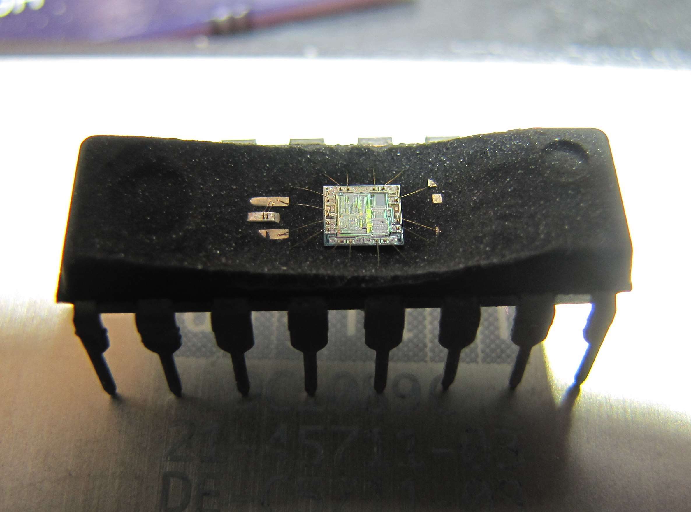


Full die image: http://retroactive.be/cic/cic_20x_die_image.jpg (Credit - Dr decap)

Using a SPI-like interface they constantly talk to each other while turned on, after exchanging the following info that is cooked into each CIC's mask ROM (there were about 14 variations):
 - Region code (NTSC / PAL)
 - "Lockout code", 5 different types

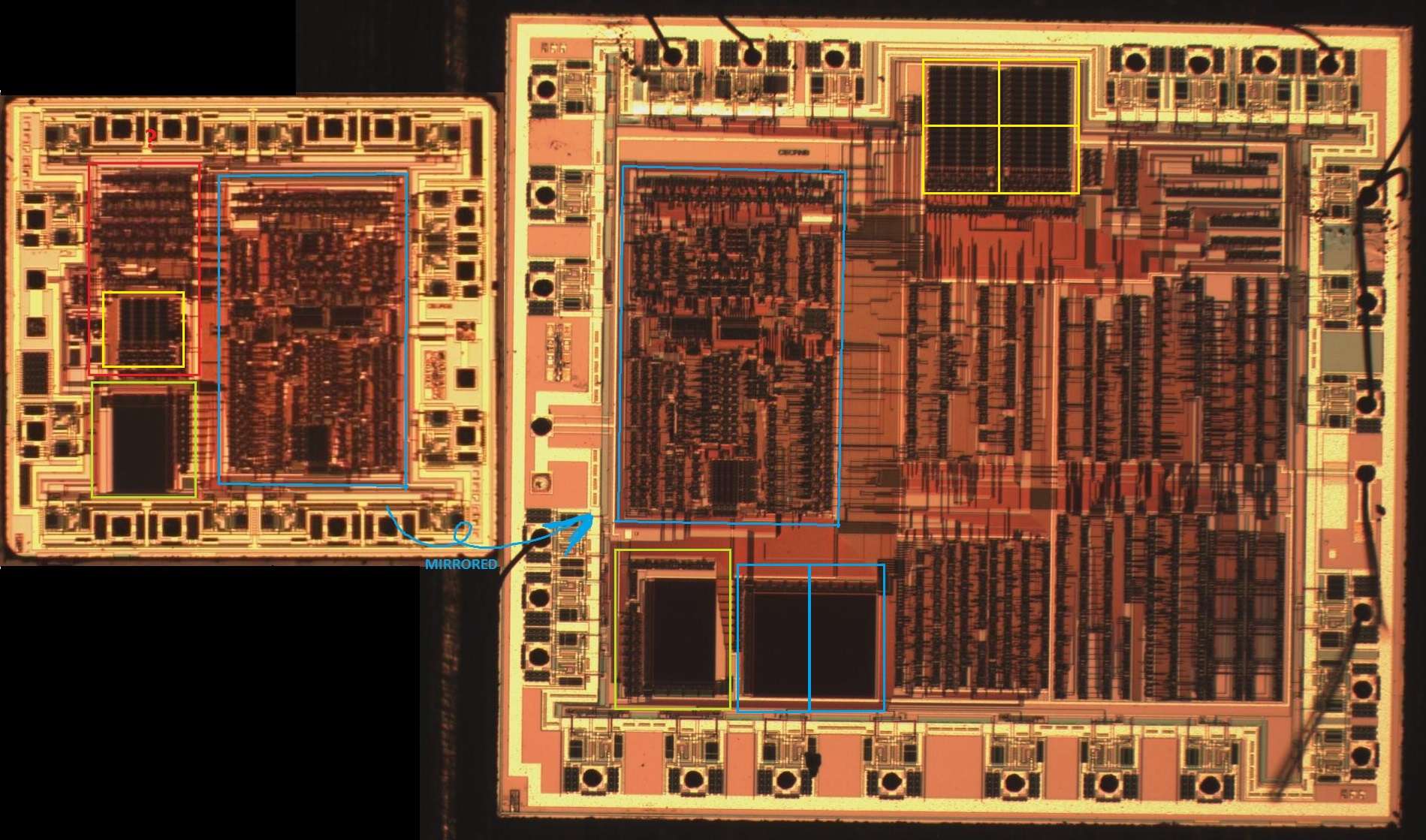
Here are the PIF and CIC dies side by side. You can see the identical SM5 cores in both (they are mirrored) sans IO in the PIF. And the right area is all the cell logic.
Bottom left are the SM5's own mask rom (yellow) and the MIPS cpu's IPL (blue)

Photo credits: Anonymous friend
« Last Edit: July 03, 2013, 02:24:31 am by marshallh »
Verilog tips
BGA soldering intro

11:37 <@ktemkin> c4757p: marshall has transcended communications media
11:37 <@ktemkin> He speaks protocols directly.
 

Offline OzOnE

  • Regular Contributor
  • *
  • Posts: 55
  • Country: gb
Re: EEVblog #491 - Nintendo 64 Game Console Teardown
« Reply #6 on: July 03, 2013, 02:54:08 am »
This is fantastic stuff, Marshall.  8)

I think that documenting every aspect of these older systems is very important.
Many of these systems still hold a lot of discoveries which need to be uncovered for accurate emulation / preservation in the future.


OzOnE.
P.S. I liked your Mask ROM decoding vid btw, keep us updated. :P
 

Offline senso

  • Frequent Contributor
  • **
  • Posts: 951
  • Country: pt
    • My AVR tutorials
Re: EEVblog #491 - Nintendo 64 Game Console Teardown
« Reply #7 on: July 03, 2013, 02:55:41 am »
And this is why this forum is so epic, post something, and like magic there is always a couple of persons that know a LOT about it.
Great info, and even better images, love to see the decaped chips  :o
 

Offline marshallh

  • Supporter
  • ****
  • Posts: 1462
  • Country: us
    • retroactive
Re: EEVblog #491 - Nintendo 64 Game Console Teardown
« Reply #8 on: July 03, 2013, 03:41:03 am »
Development carts:

Most were connected to a host comoputer via SCSI with onboard DRAM.

KMC Partner64 (sorry I can't remember the photo credits for this)


IS-Viewer (was used for development of Zelda - Ocarina of Time)


Rareware late development board.
Around late 1998 Rare contracted ALPS (they also made the 64DD expansion) to build them a more capable development board. It has a 68k on board with dual port RAM, 64mb DRAM, and SCSI connection to the host PC.
This was used for the development of Conker's Bad Fur Day and probably Perfect Dark/others.


And my own that I designed (sorry couldn't help myself :))


The console was built into the LodgeNet and "Gateway 64" inflight entertainment systems. Lodgenet offered pay per play hotels, the rom images were streamed via SCSI from a host box onto the top board. Video was transmitted over coax to the hotel room.

Photo credit: willis82


SN Systems PsyQ cart - Analog Devices cpu


Will cut this short to keep from blabbing on endlessly.
« Last Edit: July 03, 2013, 04:06:47 am by marshallh »
Verilog tips
BGA soldering intro

11:37 <@ktemkin> c4757p: marshall has transcended communications media
11:37 <@ktemkin> He speaks protocols directly.
 

Offline cloudscapes

  • Regular Contributor
  • *
  • Posts: 198
Re: EEVblog #491 - Nintendo 64 Game Console Teardown
« Reply #9 on: July 03, 2013, 03:51:24 am »
Thanks for this!

I love oldschool game console teardowns. In no small part because I actually currently work in that industry!
 

Offline Stonent

  • Super Contributor
  • ***
  • Posts: 3824
  • Country: us
Re: EEVblog #491 - Nintendo 64 Game Console Teardown
« Reply #10 on: July 03, 2013, 05:06:21 am »
Reality was an SGI branding that a number of their products had i.e.
Reality Engine: http://en.wikipedia.org/wiki/RealityEngine  (N64 is somewhat related to this)
Infinite Reality I, II and III: http://en.wikipedia.org/wiki/InfiniteReality

I had an SGI Indy that I picked up off of Ebay about 10 years ago that's in storage now
Indy R5000SC/150Mhz
128MB RAM
8bit Newport Graphics
36GB IBM UltraStar 10K (Added this one myself)

I didn't like the 8 bit graphics but never wanted to cough up the money for a 24bit board.  They also had a 3D card but it was almost never paired with the R5000 processor because the R5000 processor could do graphics calculations faster than the chip on the 3D board.

There used to be a guy known as ChicagoJoe back in the day who was building his own upgrade boards for SGI O2 workstations.  He would build boards to replace the 350MHz RM7000 chip with a BGA 600MHZ PMC Sierra RM7900 that would actually run faster than the R10000 boards.

In case anyone was interested in that cool bit of hardware hacking, it all took place here:

http://forums.nekochan.net/viewtopic.php?f=3&t=1071&start=120

« Last Edit: July 03, 2013, 05:13:14 am by Stonent »
The larger the government, the smaller the citizen.
 

Offline marshallh

  • Supporter
  • ****
  • Posts: 1462
  • Country: us
    • retroactive
Re: EEVblog #491 - Nintendo 64 Game Console Teardown
« Reply #11 on: July 03, 2013, 05:21:31 am »
I actually remember reading that a while ago. They really benefited from the die shrink.

I always did want an SGI machine but never ended up with one. Pretty inept with unix systems as well. They are very neat hardware though.
Verilog tips
BGA soldering intro

11:37 <@ktemkin> c4757p: marshall has transcended communications media
11:37 <@ktemkin> He speaks protocols directly.
 

Offline Ed.Kloonk

  • Super Contributor
  • ***
  • Posts: 4000
  • Country: au
  • Cat video aficionado
Re: EEVblog #491 - Nintendo 64 Game Console Teardown
« Reply #12 on: July 03, 2013, 05:27:40 am »
Quick (dumb) question?

Why have a 3.3v power input along with the 12v input? There's already a 5v reg on the board so why not put a 3.3v reg on there also?

iratus parum formica
 

Offline Stonent

  • Super Contributor
  • ***
  • Posts: 3824
  • Country: us
Re: EEVblog #491 - Nintendo 64 Game Console Teardown
« Reply #13 on: July 03, 2013, 05:31:06 am »
Quick (dumb) question?

Why have a 3.3v power input along with the 12v input? There's already a 5v reg on the board so why not put a 3.3v reg on there also?

Maybe they moved that to the PSU to save on heat.
The larger the government, the smaller the citizen.
 

Offline c4757p

  • Super Contributor
  • ***
  • Posts: 7799
  • Country: us
  • adieu
Re: EEVblog #491 - Nintendo 64 Game Console Teardown
« Reply #14 on: July 03, 2013, 05:33:28 am »
Because then it would be compatible with any off the shelf 12V plug.[/cynic]
No longer active here - try the IRC channel if you just can't be without me :)
 

Offline terriea

  • Contributor
  • Posts: 20
Re: EEVblog #491 - Nintendo 64 Game Console Teardown
« Reply #15 on: July 03, 2013, 10:58:46 am »

Thanks marshallh for that sweet console hardare porn ! keep it flowing !

What about the memory expansion pack ? What's inside ? Is that a simple Ram chip with a connector or there is something more ?
Does the existing packs reach the hardware limits or could we theoretically pack more RAM ?
 

Offline TacticalCode

  • Contributor
  • Posts: 16
  • Country: de
    • TacticalCode
Re: EEVblog #491 - Nintendo 64 Game Console Teardown
« Reply #16 on: July 03, 2013, 11:13:19 am »
Sweet! I can remember the day I went to Toys'r'Us (only time I've been there) with my dad to buy the N64, I must have been like 4-5 years old back then  ;D
Unfortunately we sold the N64 when we got a Gamecube, bad decision  :palm:
 

Offline Kaluriel

  • Contributor
  • Posts: 33
  • Country: 00
Re: EEVblog #491 - Nintendo 64 Game Console Teardown
« Reply #17 on: July 03, 2013, 12:45:24 pm »
Nice to see a console teardown, we should send you some more :)
 

Offline N2IXK

  • Frequent Contributor
  • **
  • Posts: 723
  • Country: us
Re: EEVblog #491 - Nintendo 64 Game Console Teardown
« Reply #18 on: July 03, 2013, 01:31:26 pm »
The non-soldered cartridge port is a good idea.

That connector sees a lot of wear and user abuse, and being able to swap it out without soldering is a big plus for serviceability.
"My favorite programming language is...SOLDER!"--Robert A. Pease
 

Offline amyk

  • Super Contributor
  • ***
  • Posts: 8420
Re: EEVblog #491 - Nintendo 64 Game Console Teardown
« Reply #19 on: July 03, 2013, 01:48:11 pm »
PIF is actually a Sharp custom labeled part. It is their own SM5 4-bit microcontroller. You take the core and slap on whatever IO you need. In this case it has 1kbyte mask rom internaly (in addition to the IPL). My theory is that all the controller polling (using a manchester encoded 1wire signal) and serial comms with the RCP glue logic is done by the huge amount of cell logic on the chip. It is like a cheap ASIC.

In the cartridges is where the CIC lives. It is also the exact same SM5 core, 1k rom with 32 nybbles of RAM.
Looks very similar to the one in the NES:
http://visual6502.org/images/pages/Nintendo_3193A.html
 

Offline Alexei.Polkhanov

  • Frequent Contributor
  • **
  • Posts: 684
  • Country: ca
Re: EEVblog #491 - Nintendo 64 Game Console Teardown
« Reply #20 on: July 03, 2013, 02:04:06 pm »
 

Offline Kernel

  • Contributor
  • Posts: 18
Re: EEVblog #491 - Nintendo 64 Game Console Teardown
« Reply #21 on: July 03, 2013, 02:17:18 pm »
From what I remember (and I have spent many many hours over the years playing N64 games) the system would not sit there 'waiting' for a cart if you turned it on without one in, after placing in the cart it was necessary to power off the system and power it back on for the game to load.
 

Offline Winston

  • Regular Contributor
  • *
  • Posts: 121
  • Country: us
    • IC Die Photography
Re: EEVblog #491 - Nintendo 64 Game Console Teardown
« Reply #22 on: July 03, 2013, 03:34:26 pm »
74hc125. Quad tristatable inverter.

The SGI logo is on both the cpu and gpu. SGI = Silicon Graphics Incorporated.
Yep. The guys that did all the gi end graphics workstations like the onyx and indi. They designed the MIPS architecture. It was their baby.
SGI was hot stuff at the time the N64 came out.  From Wikipedia:

For eight consecutive years (1995–2002), all films nominated for an Academy Award for Distinguished Achievement in Visual Effects were created on Silicon Graphics computer systems.

Conventional wisdom holds that SGI's core market has traditionally been Hollywood visual effects studios. In fact, SGI's largest revenue has always been generated by government and defense applications, energy, and scientific and technical computing. The rise of cheap yet powerful commodity workstations running Linux, Windows and Mac OS X, and the availability of diverse professional software for them, effectively pushed SGI out of the visual effects industry in all but the most niche markets, as studios adopted newer, cheaper technology.

On April 1, 2009, SGI filed for Chapter 11 again, and announced that it would sell substantially all of its assets to Rackable Systems for $25 million. The sale, ultimately for $42.5 million, was finalized on May 11, 2009.
 

Offline marshallh

  • Supporter
  • ****
  • Posts: 1462
  • Country: us
    • retroactive
Re: EEVblog #491 - Nintendo 64 Game Console Teardown
« Reply #23 on: July 03, 2013, 04:00:16 pm »
What about the memory expansion pack ? What's inside ? Is that a simple Ram chip with a connector or there is something more ?
Does the existing packs reach the hardware limits or could we theoretically pack more RAM ?

The "expansion pak" is just another 36bit rambus chip on a high density connector, with terminator resistors.
The "jumper pak" is just terminating resistors and loopbacks for the flyby serial interface and clocks.
The topology actually reminds me very much of modern day DDR3 dimms, where the address/control signals are not wired in a tree T arrangement, instead they are wired in a loop going through each part in series. Whereas the Rambus design runs the clocks serially to get around the data skew. There are two clocks so that each direction is source synchronous.
The IPL depends on the game but I believe it will loop through the initialization of each RDRAM in the chain as part of the boot process. I've booted mine with 12mb ram before (The normal max is 8mb) and it worked fine. Obviously games are coded with a fixed memory map in mind so nothing beneficial comes as a result. You're only limited by signal integrity and the distortion caused by each chip loading the bus.


74hc125. Quad tristatable inverter.
Hmm, isn't it a NON-inverting buffer? (http://www.onsemi.com/pub_link/Collateral/74HC125.REV0.PDF)
Yes, it's used as a 4bit open collector buffer, to keep the PIF inputs from blowing up if static shock is delivered to the 1wire controller interface.
4bits = 4 controllers


Looks very similar to the one in the NES:
http://visual6502.org/images/pages/Nintendo_3193A.html

It is the spiritual successor, the arch is similar but not as crusty. For example, the LFSR program counter is now a regular linear PC. However there is no stack pointerr. You just get 12bits of stack and that's it. I dumped out the rom and wrote a disassembler, but going through the code is completely horrible, with poorly named mnemonics and extremely obtuse algos. Writing PIC assembly is like coding high level Java compared to this.

« Last Edit: July 03, 2013, 04:03:43 pm by marshallh »
Verilog tips
BGA soldering intro

11:37 <@ktemkin> c4757p: marshall has transcended communications media
11:37 <@ktemkin> He speaks protocols directly.
 

Offline adam1213

  • Regular Contributor
  • *
  • Posts: 120
  • Country: au


Share me

Digg  Facebook  SlashDot  Delicious  Technorati  Twitter  Google  Yahoo
Smf