Author Topic: Z80 Data, Address & Control signal buffering/driving design. Is this design ok?  (Read 4600 times)

0 Members and 1 Guest are viewing this topic.

Offline castingflameTopic starter

  • Regular Contributor
  • *
  • Posts: 100
  • Country: gb
I wish to design a better way of connecting to my Z80 based machines to enable me to play around with the Z80 in a much safer way.

Additionally, I will be using ribbon cables from each machine to my breadboard. My idea is to have a small PCB on the port of my machine with, the circuit show below, to introduce buffers to help 'drive' the signal over the ribbon cable and to create some safety margin from killing my machine (again!).


This is what I have come up with so far ...


I may well use HCT instead of LS because of the lower power consumption but not sure why else it is a good or bad idea with that one.


What do you think?
« Last Edit: September 25, 2019, 10:53:23 am by castingflame »
 

Offline TomS_

  • Frequent Contributor
  • **
  • Posts: 851
  • Country: gb
You're going to need to change the LS32 (OR) to an 08 (AND), since you can't be doing both IORQ and MREQ at the same time, so the output would always be high and never enable the buffer for the data bus.

Other concerns will be around additional delays introduced by the buffers, and whether that will present issues for any existing logic. If this is an older retro style computer system that shares memory between CPU and video for example, will your timing still be valid with another 10ns of delay added in.

Perhaps adding a pull down resistor pack between the Z80 and data buffer so that those pins are never floating when everything is tri-stated would be a good idea.

Otherwise ... The only other thing I can think of is what issues you are trying to protect against by fully buffering the CPU?
« Last Edit: September 25, 2019, 01:28:11 pm by TomS_ »
 
The following users thanked this post: castingflame

Offline TomS_

  • Frequent Contributor
  • **
  • Posts: 851
  • Country: gb
Also, you may also want to reverse the direction of some of the signals you are buffering, so that they can be manipulated from your breadboard. Or maybe dont buffer them at all and use an open collector/drain type interface to control them.

e.g. the RESET, BUSRQ, INT, NMI and WAIT signals are all inputs to the Z80 which you can interact with from an external board. e.g. you may want to pull WAIT low while a peripheral does something, or you may want to generate an interrupt, or may want to pull BUSRQ low so that you can take over the bus. But in particular for the latter to happen, you'll also need to reverse the direction of the address bus and also the data bus buffer which will require a bit more logic to achieve. I guess it depends what you want to do from your breadboard.
 
The following users thanked this post: castingflame

Offline Ian.M

  • Super Contributor
  • ***
  • Posts: 13139
Your data bus buffer absolutely will not work, even with TomS's proposed change.  You can do that sort of thing with a bare Z80, but if its in a system with any RAM, ROM, or I/O on the CPU side of the buffer, it will cause bus contention.   You need to decode the memory or I/O address range for your breadboard, which *MUST* *NOT* clash with any used address range on the CPU side, and, during read cycles gate the buffer enable with the decoded address.   If you don't get the access timing exact or make a mistake with the memory decoding, and are using 74HC/HCT logic, 330R resistors in series with all the databus lines on the CPU side will prevent bus contention causing any physical damage.
 
The following users thanked this post: TomS_, castingflame

Offline castingflameTopic starter

  • Regular Contributor
  • *
  • Posts: 100
  • Country: gb
Firstly thank you for answering, it gave me plenty more things to think about. I will do a point by point response in hope to keep things clear  (for mainly my benefit).

Initial Requirements [After reading your comments]
Initially I want something that will enable me to use my ZX Spectrum for port I/O. I will need access to the full address bus for 16bit address decoding. I am aware that normally only the lower 8 bits of the address bus is used but the spectrum does have the ability to address/and uses the full 16bit addresses in some hardware. I will not be adding anything like RAM or ROM etc just port I/O.

Quote
You're going to need to change the LS32 (OR) to an 08 (AND), since you can't be doing both IORQ and MREQ at the same time, so the output would always be high and never enable the buffer for the data bus.

If I am only concerned with IO, can I get away with just IORQ as a CS for the data bus buffer?

Quote
Other concerns will be around additional delays introduced by the buffers, and whether that will present issues for any existing logic. If this is an older retro style computer system that shares memory between CPU and video for example, will your timing still be valid with another 10ns of delay added in

I understand what you are saying but if I just stick with port I/O will this be a problem?


Quote
Perhaps adding a pull down resistor pack between the Z80 and data buffer so that those pins are never floating when everything is tri-stated would be a good idea. Otherwise ... The only other thing I can think of is what issues you are trying to protect against by fully buffering the CPU?

I want to use some LEDs on address, data & control lines. I understand they are fast but I will also use this for single stepping another project. With  that in mind I was going to just put the LEDs on the other side of a  buffer on their own but as I am using a ribbon cable from the Speccy I thought it would be a good idea to put them on the other end on the cable next to the Speccy to help drive the signal across the ribbon cable and provide enough current and isolation from directly connecting my 'self educating' rough designs directly to my Speccy. If I got things stupidly wrong for some reason (again!) the buffer should protect the Speccy. That was my idea. Is this reasonable or stupid?!


Quote
... you'll also need to reverse the direction of the address bus and also the data bus buffer which will require a bit more logic to achieve. I guess it depends what you want to do from your breadboard.

I believed that my RD on my Data Bus buffer, when 'inactive,' was supposed to indicate a WR. Thinking about it more I will need to bring WR to that pin with some additional logic too so the pin is actively changed to 1 to change direction of the buffer. I'll redesign.


Will this basic design need a bi-directional address bus as I will only be using the address bus for decoding and not placing anything on it for other ICs to read?

Quote
Also, you may also want to reverse the direction of some of the signals you are buffering, so that they can be manipulated from your breadboard. Or maybe dont buffer them at all and use an open collector/drain type interface to control them.

I'll look into that. Any suggestions?


Quote
Your data bus buffer absolutely will not work, even with TomS's proposed change.  You can do that sort of thing with a bare Z80, but if its in a system with any RAM, ROM, or I/O on the CPU side of the buffer, it will cause bus contention.   You need to decode the memory or I/O address range for your breadboard, which *MUST* *NOT* clash with any used address range on the CPU side, and, during read cycles gate the buffer enable with the decoded address.   If you don't get the access timing exact or make a mistake with the memory decoding, and are using 74HC/HCT logic, 330R resistors in series with all the data bus lines on the CPU side will prevent bus contention causing any physical damage.

As stated above I was going to just use port IO. Is there any reason why I can not put my decoding on my breadboard, downstream of the buffer? Nothing will be put on the data bus until all the correct address and control signal decoding is done, say with a 74LS138. It will not be the 138 but it is an example.

As for I/O addresses, I know what I can and can not use, so that is not a problem. I have that bit mapped out.

330R resistors sounds like a very good idea. Will they go in front of the buffers?


I will spend some more time in the morning updating the schematic. I will include the decoding to see if it is correct.


TomS_  &  Ian.M      I really appreciate you help. As you can tell, I am still learning. :-+
« Last Edit: September 25, 2019, 09:25:05 pm by castingflame »
 

Offline Ian.M

  • Super Contributor
  • ***
  • Posts: 13139
ZX Spectrums have minimalist I/O address decoding.   The original rubber key 16K/48K and the ZX Spectrum+ models had no address decoding whatsoever and simply used Z80 address line A0 as the ULA chip select.   Later models kept the A0 ULA /CS for compatibility and added partial address decoding for their new hardware functions using A1 as /CS.  This means that many I/O addresses are forbidden and will cause contention if used for external peripherals.  As 'short' Z80 I/O addresses are only 8 bit, if you have extra devices like Interface 1 on a rubber key speccy, there are only five low byte address lines left, which vastly complicates interfacing peripherals that need several address lines + a decoded /CS.  If you need your hardware to be safe plugged into any speccy, you must avoid any address with A4, A3, A1 or A0 low.

See https://www.worldofspectrum.org/faq/reference/ports.htm

LEDs on the un-decoded address, and data and control bus are essentially worthless on any Z80 system where you  cant stop the clock (e.g. a ZX speccy, because it uses DRAM refreshed by the Z80, so stopping it crashes the system within a few ms) as the refresh cycle will cause activity on A14:A0 .   OTOH if you use transparent latches to drive the LEDs, and decode a suitable gate signal for the latches, you can get a useful indication.

If your breadboard device is 'write only' i.e. never responds on the data bus and doesn't assert any Z80 control lines, you can put all decoding after a unidirectional output only buffer.

However if you need to read bytes from your breadboard device, you *MUST* have enough address decoding in front of the buffer's output enable to avoid contention when the direction control selects it for input.   If on a ZX Speccy any of the address lines I mentioned earlier are low, the buffer *MUST* be disabled. 
 

Offline TomS_

  • Frequent Contributor
  • **
  • Posts: 851
  • Country: gb

If I am only concerned with IO, can I get away with just IORQ as a CS for the data bus buffer?

By doing that you will be essentially assigning the entire IO address space to your breadboard. I think Ian.M has covered that topic quite well.


Quote

I understand what you are saying but if I just stick with port I/O will this be a problem?

If you're only paying with IO then I think you should be fine.

Quote
I want to use some LEDs on address, data & control lines. I understand they are fast but I will also use this for single stepping another project. With  that in mind I was going to just put the LEDs on the other side of a  buffer on their own but as I am using a ribbon cable from the Speccy I thought it would be a good idea to put them on the other end on the cable next to the Speccy to help drive the signal across the ribbon cable and provide enough current and isolation from directly connecting my 'self educating' rough designs directly to my Speccy. If I got things stupidly wrong for some reason (again!) the buffer should protect the Speccy. That was my idea. Is this reasonable or stupid?!

Beware of DRAMs which need to be refreshed, Ian.M also covered that. If the system uses DRAM then you won't be able to slow it down enough to make LED indicators useable. Of the system could be modified to use SRAM then you're in with a shot.

Quote

I believed that my RD on my Data Bus buffer, when 'inactive,' was supposed to indicate a WR. Thinking about it more I will need to bring WR to that pin with some additional logic too so the pin is actively changed to 1 to change direction of the buffer. I'll redesign.

IIRC you can use a high (inactive) RD signal in combination with a chip select signal to indicate a write operation. The 68k uses a single pin to differentiate this way. You shouldn't need to bring WR to that buffer, but got are going to need to think carefully about how your breadboarded peripherals will access the data bus. E.g. if they take over from the CPU (ala BUSRQ) then the read direction is effectively reversed. Lots to think about in that respect. :-)

Quote

Will this basic design need a bi-directional address bus as I will only be using the address bus for decoding and not placing anything on it for other ICs to read?

Only if the peripheral is going to take over the buses and drive those signals.

Quote

I'll look into that. Any suggestions?

That was my suggestion. :-) I suppose it depends on what exactly you want to do on your breadboard.

Don't forget, you might also be fine simply adding some current limiting resistors in line with your external design, as long as you're sticking with logic level voltages then the worst you might do is crash it perhaps by causing data corruption through bus contention, but physical damage should be avoided due to limited current (i.e. no need to worry about two chips driving opposite polarities and sorting reach other out). I think Ian.M also touched on this in one of his posts.
 

Offline castingflameTopic starter

  • Regular Contributor
  • *
  • Posts: 100
  • Country: gb
Quote
ZX Spectrums have minimalist I/O address decoding.   The original rubber key 16K/48K and the ZX Spectrum+ models had no address decoding whatsoever and simply used Z80 address line A0 as the ULA chip select.   Later models kept the A0 ULA /CS for compatibility and added partial address decoding for their new hardware functions using A1 as /CS.  This means that many I/O addresses are forbidden and will cause contention if used for external peripherals.  As 'short' Z80 I/O addresses are only 8 bit, if you have extra devices like Interface 1 on a rubber key speccy, there are only five low byte address lines left, which vastly complicates interfacing peripherals that need several address lines + a decoded /CS.  If you need your hardware to be safe plugged into any speccy, you must avoid any address with A4, A3, A1 or A0 low.

Completely agree.  Initially I will make sure this 'bread boarding design' (not my interface)  is working okay with a 74LS138 and just use an existing port like $1F (Kempston 1) to test that everything is working okay. I will then exchange this for a CPLD and use all 16 address bits & required control signals. As I am new to CPLD, apart from a few fundamental experiments,  I wanted to get my design proved working with partial decoding first, one step at a time.


Quote
LEDs on the un-decoded address, and data and control bus are essentially worthless on any Z80 system where you  cant stop the clock (e.g. a ZX speccy, because it uses DRAM refreshed by the Z80, so stopping it crashes the system within a few ms) as the refresh cycle will cause activity on A14:A0 .   OTOH if you use transparent latches to drive the LEDs, and decode a suitable gate signal for the latches, you can get a useful indication.

Yes I did wonder about the refresh cycle so I was going to replace my DRAMs with SRAMs like these replacement modules ...

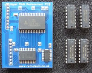


Actually as I type this I just got a notification of a update to this post and read that Tom actually recommends SRAM too. Hopefully this is correct then.

As the ULA provides the clock for the Z80 on the Speccy, I was unsure if I would be able to slow down the speccy enough, without it effecting 'other stuff', to make looking at the signals via LEDs waste of time or not.

There are 2 additional reasons I thought about using LEDs;

1) So that I can use this same design on other boards like my RC2014 etc that do have the ability to single step
2) Fault finding a dodgy Speccy for stuck bits on faulty DRAMs.


OTOH
Maybe a better approach is to forget about the above and to narrow my focus and make this breadboard design just for the Speccy and my current project using port I/O. With that in mind, it may be a better idea to forget about the Address & Data LEDs and just use LEDs on the control bus as this will at least give me useful information I can see with the speccy running at full speed.


Quote
If your breadboard device is 'write only' i.e. never responds on the data bus and doesn't assert any Z80 control lines, you can put all decoding after a unidirectional output only buffer.

However if you need to read bytes from your breadboard device, you *MUST* have enough address decoding in front of the buffer's output enable to avoid contention when the direction control selects it for input.   If on a ZX Speccy any of the address lines I mentioned earlier are low, the buffer *MUST* be disabled.

Thank you, I understand what you mean a little better so I will need decoding first.


Summing Up
Narrow my focus to this project only. I guess my main priority is wanting to keep my Speccy alive while still learning. After that I would like some indication, via LEDs of what is going on with my circuit.


With this in mind maybe a better approach is to;

1) Just use current limiting resistors on the lines for protection against myself and forget buffers altogether.
2) Decode the address lines after the limiting resistors. Initially with a 74LS138 then later CPLD.
3) Check correct design for RD/WR IORQ M1 etc with address lines to activate the decoder.
4) Use a driver for the control signal LEDs. Maybe ULN darlington type. Will investigate.


Better?


Thanks again, really appreciate  :-+

« Last Edit: September 26, 2019, 09:56:10 am by castingflame »
 

Offline TomS_

  • Frequent Contributor
  • **
  • Posts: 851
  • Country: gb
Actually as I type this I just got a notification of a update to this post and read that Tom actually recommends SRAM too. Hopefully this is correct then.

SRAM, being static, doesnt need to be refreshed periodically, so you can stop the CPU clock completely, ignore the RFSH signal entirely (I actually hook the RFSH signal up to the active high input of a '138 to make sure no device is selected during a refresh cycle in my designs because I only work with SRAM), and the RAM will hold its contents as long as it has power. Hence why it is also used for battery backed RAM applications.

Some CPUs use dynamic registers internally, e.g. the 68k, so you cant stop the clock to them or their registers lose contents as well. Theres a good video on YouTube that shows you how you can single step a 68k without stopping the clock, which basically involves fooling it into thinking that the device it is reading from hasnt yet placed the requested data onto the data bus.

But the Z80 has static registers, so that isnt a problem for it.

Quote
3) Check correct design for RD/WR IORQ M1 etc with address lines to activate the decoder.
You might find something like http://logic.ly helpful in working that out. Ive used it quite a few times, its good for visualising your logic. They have a free demo on their website, but you cant save your work. I think you can also download a free trial of their desktop software.

Quote
4) Use a driver for the control signal LEDs. Maybe ULN darlington type. Will investigate.
You shouldnt necessarily need anything like that. You could use some inverters or something, minimal load on the signals and the outputs can sink or source to drive the LEDs.
 
The following users thanked this post: castingflame

Offline castingflameTopic starter

  • Regular Contributor
  • *
  • Posts: 100
  • Country: gb
Great Info thank you Tom!

I have since found out that the Z80 only has a capability of 'Standard TTL Load' on each pin which is 1.6mA (apparently!) so I 100% will need something to drive the LEDs. <<< This statement is for my benefit :)


I am only looking at running the 5 (control bus) LEDs at around maybe 10mA so things like the ULNxxx darlington drivers look complete overkill. I then thought about small FETs or even standard switching transistors. However, I much prefer your idea of inverters. It seems cleaner and less 'welly'on the lines. Thank you.


SPICE
I have always had on my list to learn about SPICE modelling and today I was going to actually pull my finger out and do it. Like you have said, this seems like a good excuse to be able to visually see what is going on better. I will take a look at http://logic.ly  and my installed SPICE app so thank you for your suggestion  :-+


Quote
... RFSH signal up to the active high input of a '138 to make sure no device is selected during a refresh cycle in my designs because I only work with SRAM

Very clever!


I will get my circuit into some sort of modelling before coming back this time so it may take a day or too.


Thanks again.


Offline TomS_

  • Frequent Contributor
  • **
  • Posts: 851
  • Country: gb
Great Info thank you Tom!

I have since found out that the Z80 only has a capability of 'Standard TTL Load' on each pin which is 1.6mA (apparently!) so I 100% will need something to drive the LEDs. <<< This statement is for my benefit :)

You dont need much to drive modern LEDs - a couple of mA is plenty. Ive even used 3.3K resistors on a 3.3V supply to drive some LEDs with very respectable output. It will all depend on the LEDs you have. Play around with some values (1K+), you'll probably find that you dont need anywhere near 10's of mA or any special drivers.

But I guess you dont really want to be loading your signals down just to drive an LED, so buffering them through something else is still a good idea.
 
The following users thanked this post: castingflame

Offline Ian.M

  • Super Contributor
  • ***
  • Posts: 13139
On 'classic' ZX speccys, the clock output on the edge connector is very low level, IIRC under 1V pk-pk.   I *think* its also inverted with respect to the Z80 clock pin.  If you need it for any peripheral chips (e.g. Z80 PIO, CTC etc.), you'll have to regenerate it.   The easiest option is to AC couple it into a carefully biassed fast inverter, then put it through a couple more direct coupled inverter stages to square it up.


Due to the Z80's fanout limitations, and the fact its already driving the ULA and two banks of DRAM (assuming 48K model) its preferable to use 74HCT logic, not LS TTL, for its lower loading on the signals.
 
The following users thanked this post: castingflame

Offline TomS_

  • Frequent Contributor
  • **
  • Posts: 851
  • Country: gb
On 'classic' ZX speccys, the clock output on the edge connector is very low level, IIRC under 1V pk-pk.   I *think* its also inverted with respect to the Z80 clock pin.  If you need it for any peripheral chips (e.g. Z80 PIO, CTC etc.), you'll have to regenerate it.   The easiest option is to AC couple it into a carefully biassed fast inverter, then put it through a couple more direct coupled inverter stages to square it up.


Due to the Z80's fanout limitations, and the fact its already driving the ULA and two banks of DRAM (assuming 48K model) its preferable to use 74HCT logic, not LS TTL, for its lower loading on the signals.

I dont really know anything about the ZX Spectrum, so I went and had a look and it does indeed look like the clock signal on the edge connector will be inverse to what the CPU sees. The CPU clock pin is driven by an open collector circuit, and the signal from the ULA which drives that transistor (PHICPU) is presented on the edge connector.
 
The following users thanked this post: castingflame


Share me

Digg  Facebook  SlashDot  Delicious  Technorati  Twitter  Google  Yahoo
Smf