A couple of photos, as promised (click on image for slightly larger version)
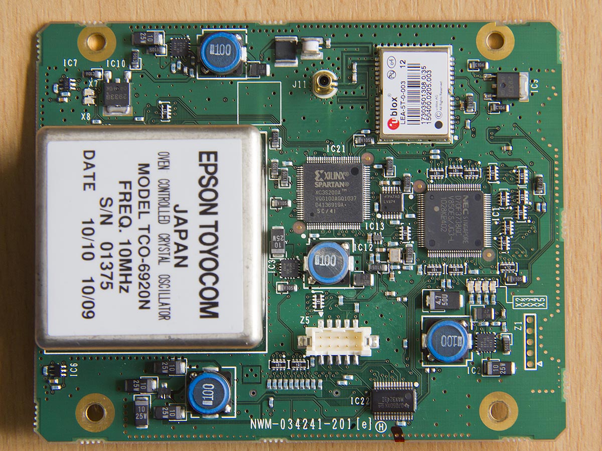
Top of board:

The GPS module is a ublox LEA-5T with what looks to be an SNB RF connector, the white connector has traces going to a max3243 (just below/right of Z5) so I presume carries a serial interface. The blue inductor and four caps at the bottom left are DC supply filtering, the three other inductors are part of separate DC-DC converters built around the tps62110 step-down converter and there are a couple of 3.3V regulators top right & top left. There's also a Xilinx XC3S200A FPGA, presumably for glue logic.
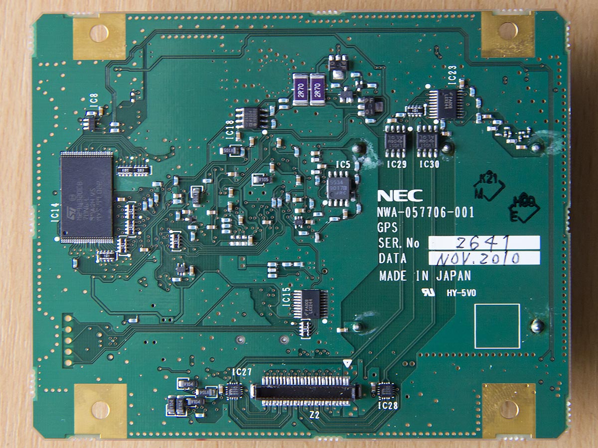
Bottom of board:

This looks interesting, the first thing I noticed was several differential tracks running to the connector at the bottom of the board - these run to two Micrel SY89833 LVDS fanout buffers - these have a 2GHz bandwidth and claim < 190ps rise and fall times so the 10MHz out is going to have
sharp edges! The inputs to the fan-out buffers come from a further pair of LVDS buffers, in this case the TI LVDS104M. Actually I'm slightly puzzled here. The datasheet for the LVDS104 says it is a 16 pin part, but there are 8 pin parts on the board. They are clearly marked with the TI logo and LVDS104M but I can't find this part on the TI web site - does anyone have any pointers?
The OCXO output itself runs through what looks like some LC filtering, then to a 74LCX244 buffer, then presumably into the LVDS104's
As well as the LVDS outputs the bottom connector has DC in - presumably 12V as it runs straight through to the OCXO VCC pin with just a bit of LC decoupling. there are also 15 lines on the opposite side to the LVDS output, most of these have 10k pulls downs attached (the row of SMD resistors below Z5 on the top of the board). It is not possible to trace them visually into the board after that so they could run up to the FPGS or the CPU - no idea whether they are a parallel interface or status lines or what.
Finally there are four TTL level lines running out to the unpopulated connector Z1, not sure what these are - some sort of serial debug interface (not JTAG as not enough pins).
I might power it later today and check that the 3.3V logic gets power with just 12V applied, I can't try it out properly until I get hold of a SNB to BNC adapter to hook it up to the GPS antenna.
UPDATE: Powered up, various LEDs flash & change so the processor is probably OK and 10MHz out of one set of LVDS outputs, so the OCXO is working (and the oven current conforms to the datasheet). The other set is inactive, there is nothing out of one of the LVDS104M's - but I don't know whether that's because of a fault or it's supposed to do that.
Datasheets
OCXO:
http://www.wild-pc.co.uk/docs/TCO-6920N.pdfCPU:
http://media.digikey.com/pdf/Data%20Sheets/Renesas/uPD70F3737,38,92,93.pdfRS232:
http://www.ti.com/lit/ds/symlink/max3243.pdfGPS:
http://www.u-blox.com/images/downloads/Product_Docs/LEA-5_NEO-5_TIM-5H_HardwareIntegrationManual%28GPS.G5-MS5-09027%29.pdfDC-DC:
http://www.ti.com/lit/ds/symlink/tps62110.pdfFPGA:
http://www.xilinx.com/support/documentation/data_sheets/ds529.pdfLVDS:
http://www.micrel.com/_PDF/HBW/sy89833al.pdf http://www.ti.com/lit/ds/slls396f/slls396f.pdf