Author Topic: Plane Clearance on Non Round pads - Designer 10.589  (Read 2336 times)

0 Members and 1 Guest are viewing this topic.

Offline envisionelecTopic starter

  • Frequent Contributor
  • **
  • Posts: 286
  • Country: us
Plane Clearance on Non Round pads - Designer 10.589
« on: September 20, 2013, 10:33:04 pm »
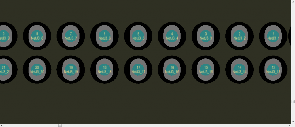
I have a bit of an issue I've not encountered before. The Internal Plane clearance doesn't seem to avoid non-round pads properly. I have to enlarge the spacing to ridiculous proportions to clear the pads. I don't recall having this problem previously, but that might be because I almost never use through hole parts.

I tried fixing it in DRE like InPolygon (but InPlane, instead). I mustn't have the correct syntax as I got an error.

I can split the plane around the connectors I don't want affected. But is there a more elegant solution?

My Google-Fu is weak tonight, I guess.  :-//


Offline marshallh

  • Supporter
  • ****
  • Posts: 1462
  • Country: us
    • retroactive
Re: Plane Clearance on Non Round pads - Designer 10.589
« Reply #1 on: September 20, 2013, 10:48:02 pm »
Go into 3d view and fly inside the board. I'll bet you'll find that the inner rings are perfect circles, not ovals like the outer layers.
Verilog tips
BGA soldering intro

11:37 <@ktemkin> c4757p: marshall has transcended communications media
11:37 <@ktemkin> He speaks protocols directly.
 

Offline envisionelecTopic starter

  • Frequent Contributor
  • **
  • Posts: 286
  • Country: us
Re: Plane Clearance on Non Round pads - Designer 10.589
« Reply #2 on: September 20, 2013, 11:00:17 pm »
Go into 3d view and fly inside the board. I'll bet you'll find that the inner rings are perfect circles, not ovals like the outer layers.

Ah - of course. I didn't even have to do this to know you're exactly right.

Man...some days I'm a real moron. Hahah.


Share me

Digg  Facebook  SlashDot  Delicious  Technorati  Twitter  Google  Yahoo
Smf